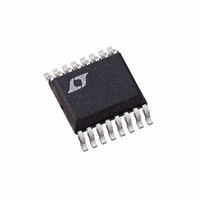
LT4220CGN Linear Technology, LT4220CGN Datasheet - Page 10

LT4220CGN
Manufacturer Part Number
LT4220CGN
Description
IC CNTRLR DUAL HOT SWAP 16-SSOP
Manufacturer
Linear Technology
Type
Hot-Swap Controllerr
Datasheet
1.LT4220CGNPBF.pdf
(16 pages)
Specifications of LT4220CGN
Applications
General Purpose
Internal Switch(s)
No
Voltage - Supply
2.7 V ~ 16.5 V
Operating Temperature
0°C ~ 70°C
Mounting Type
Surface Mount
Package / Case
16-SSOP (0.150", 3.90mm Width)
Lead Free Status / RoHS Status
Contains lead / RoHS non-compliant
Available stocks
Company
Part Number
Manufacturer
Quantity
Price
Company:
Part Number:
LT4220CGN
Manufacturer:
LT
Quantity:
10 000
Part Number:
LT4220CGN
Manufacturer:
LTNEAR
Quantity:
20 000
Part Number:
LT4220CGN#PBF
Manufacturer:
LINEAR/凌特
Quantity:
20 000
Part Number:
LT4220CGN#TRPBF
Manufacturer:
LINEAR/凌特
Quantity:
20 000
LT4220
TI I G DIAGRA S
APPLICATIO S I FOR ATIO
Hot Circuit Insertion
When circuit boards are inserted into a live backplane, the
circuit board bypass capacitors can draw large peak
currents from the backplane power bus as they charge up.
The LT4220 is designed to turn on a board’s V dual
supplies in a controlled manner, allowing the circuit board
to be safely inserted or removed from a live backplane. The
part provides supply tracking as well as undervoltage and
overcurrent protection. Power good and fault output sig-
nals indicate, respectively, if both power output voltages
are ready or if an overcurrent time-out fault has occurred.
10
W U
GATE
GATE
ON
ON
V
0V
–
–
EE
0V
0V
+
+
V
CC
– SENSE
Figure 5. SENSE
GATE
Figure 1. ON
Figure 3. ON
1V
–1V
0V
+
+
U
V
0.5V
t
EE
PLHON
t
PLHON +
+ 1.2V
50mV
–
+
–
U
-to-GATE
-to-GATE
+
W
-to-GATE
10V
t
SENSE +
+
V
–
W
–1V
EE
Timing
1V
Timing
+
+ 3.5V
Timing
4220 F05
10V
100mV
0V
100mV
4220 F03
4220 F01
t
PHLON
U
t
PHLON +
–
The dual power supply on the circuit board is controlled
with two external N-channel pass transistors Q1 and Q2 in
the V dual power supply path. The sense resistors R
and R
C2 control the V
TRACK pin can be tied to V
voltages to ramp up together by tracking the voltages at
the FB
control loop compensation while R5 and R7 prevent high
frequency oscillations in Q1 and Q2. C3 and R8 on Q2
prevent fast dV/dt transients from turning Q2 on during
PWRGD
PWRGD
S
+
–
FB
and FB
FB
provide current detection while capacitor C1 and
0V
0V
+
V
0V
0V
–
EE
– SENSE
GATE
Figure 6. SENSE
–
Figure 2. FB
Figure 4. FB
pins. Resistors R6 and R8 provide current
OUT
1V
–1V
0V
–
–
+
2.5V
2.5V
and V
t
t
PLHFB +
PLHFB
–50mV
+
–
–
-to-PWRGD Timing
-to-PWRGD Timing
OUT
–
CC
–2V
-to-GATE
t
SENSE
–
enabling the dual output
slew rate. Optionally, the
–
–1V
1V
–
Timing
2.5V
4220 F06
2.5V
–100mV
V
100mV
EE
4220 F02
4220 F04
t
t
PHLFB +
PHLFB
–
4220f
S
+


