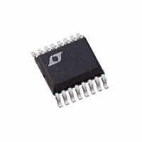
LT4220CGN Linear Technology, LT4220CGN Datasheet - Page 13

LT4220CGN
Manufacturer Part Number
LT4220CGN
Description
IC CNTRLR DUAL HOT SWAP 16-SSOP
Manufacturer
Linear Technology
Type
Hot-Swap Controllerr
Datasheet
1.LT4220CGNPBF.pdf
(16 pages)
Specifications of LT4220CGN
Applications
General Purpose
Internal Switch(s)
No
Voltage - Supply
2.7 V ~ 16.5 V
Operating Temperature
0°C ~ 70°C
Mounting Type
Surface Mount
Package / Case
16-SSOP (0.150", 3.90mm Width)
Lead Free Status / RoHS Status
Contains lead / RoHS non-compliant
Available stocks
Company
Part Number
Manufacturer
Quantity
Price
Company:
Part Number:
LT4220CGN
Manufacturer:
LT
Quantity:
10 000
Part Number:
LT4220CGN
Manufacturer:
LTNEAR
Quantity:
20 000
Part Number:
LT4220CGN#PBF
Manufacturer:
LINEAR/凌特
Quantity:
20 000
Part Number:
LT4220CGN#TRPBF
Manufacturer:
LINEAR/凌特
Quantity:
20 000
APPLICATIO S I FOR ATIO
Current Limit/Electronic Circuit Breaker
The LT4220 features foldback current limit with an elec-
tronic circuit breaker that protects against short-circuits
or excessive supply currents. The current limit is set by
placing sense resistors between V
(Pin 15) and between SENSEK (Pin 2) and SENSE
An adjustable timer will trip an electronic circuit breaker if
the part remains in current limit for too long.
To prevent excessive power dissipation in the pass tran-
sistors and to prevent voltage spikes on the input supply
during overcurrent conditions at the output, the current
folds back as a function of the output voltage, which is
sensed at the feedback pins FB
at the FB
15mV (–15mV), and limits the current to I
R
sense amplifier offset increases until the FB
voltage reaches 0.85V (–0.75V), At which point the cur-
rent limit reaches a maximum of I
(– 52mV/R
Timer Function and Autorestart
The TIMER pin (Pin 8) provides a method for setting the
maximum time the LT4220 is allowed to operate in current
limit. When the current limit circuitry is not active, the
TIMER pin is pulled to GND by a 3.3 A current sink.
Whenever the current limit circuit becomes active, by
either a positive or negative sense amplifier operating in
current limit, a 65 A pull-up current source is connected
to the TIMER pin and the voltage rises with a slope equal
to dV/dt = 65 A/C
can be set with a capacitor value of:
If the current limit circuit turns off, the TIMER pin will be
discharged to GND at a rate of:
Whenever the TIMER pin ramps up and reaches the 1.24V
threshold, the internal fault latch is set and the FAULT pin
(Pin 11) is pulled low. GATE
GATE
ramping back to GND by the 3.3 A current sink. After the
S
+
C
dV/dt = 3.3 A/C
TIMER
(–15mV/R
–
is pulled down to V
+
= t • 65 A/1.24V
(or FB
S
–
).
S
–
–
). As the output voltage increases, the
) pin is 0V, the sense amplifier offset is
TIMER
TIMER
U
. The desired current limit time (t)
U
EE
+
+
, and the TIMER pin starts
is pulled down to ground,
and FB
CC
W
(Pin 16) and SENSE
–
LIMIT
. When the voltage
LIMIT
= 48mV/R
U
+
–
= 15mV/
(or FB
(Pin 3).
(4)
(5)
S
–
+
+
)
fault latch is set, the LT4220 can be restarted by pulling the
ON
LT4220 can also be restarted by cycling either supply
beyond its UVLO. Otherwise the part remains latched off.
For autorestart, the FAULT pin can be tied to the ON
The autorestart will occur after the TIMER pin falls below
0.5V.
Undervoltage Detection
The ON
condition at the power supply inputs. The ON
pins are connected to analog comparators with 50mV of
hysteresis. If the ON
or the ON
pins are pulled low and held low until the ON
exceed their turn-on thresholds (1.24V and –1.24V). Ex-
ternal capacitance at the ON pins may be required to filter
supply ringing from crossing the ON comparator thresh-
old.
Additionally there is an internal undervoltage lockout on
both supplies of approximately V
–2.45V. If either supply is in UVLO, both GATE pins will be
pulled low and all internal latches will be reset.
ON
If the ON
negative supply through a resistor divider, a 10k resistor
must be connected between the driver and the ON
Power Good Detection
The LT4220 includes two comparators for monitoring the
output voltages. The FB
against 1.24V and –1.24V internal references respectively.
The comparators exhibit 50mV of hysteresis. The com-
parator outputs are wire-ORed to the open collector PWRGD
pin that is enabled once both GATE
reached their maximum gate drive voltage as indicated by
the internal gate good latches. The PWRGD pin goes high
impedance when both FB
and V
has been fully on.
+
–
Protection
pin low after the TIMER pin falls below 0.5V. The
FB
+
–
and ON
–
H
–
pin is driven directly and not connected to the
thresholds, GATE
pin rises above its threshold voltage, the GATE
–
pins can be used to detect an undervoltage
+
pin falls below its threshold voltage
+
and the FB
+
and FB
+
is fully on and Gate
CC
+
–
and GATE
inputs exceed V
–
< 2.45V and V
pins are compared
+
LT4220
and ON
–
+
pins have
and ON
–
13
initially
–
–
+
pin.
FB
pins
EE
pin.
4220f
+
>
H
–


