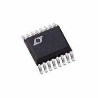
LT4220CGN Linear Technology, LT4220CGN Datasheet - Page 8

LT4220CGN
Manufacturer Part Number
LT4220CGN
Description
IC CNTRLR DUAL HOT SWAP 16-SSOP
Manufacturer
Linear Technology
Type
Hot-Swap Controllerr
Datasheet
1.LT4220CGNPBF.pdf
(16 pages)
Specifications of LT4220CGN
Applications
General Purpose
Internal Switch(s)
No
Voltage - Supply
2.7 V ~ 16.5 V
Operating Temperature
0°C ~ 70°C
Mounting Type
Surface Mount
Package / Case
16-SSOP (0.150", 3.90mm Width)
Lead Free Status / RoHS Status
Contains lead / RoHS non-compliant
Available stocks
Company
Part Number
Manufacturer
Quantity
Price
Company:
Part Number:
LT4220CGN
Manufacturer:
LT
Quantity:
10 000
Part Number:
LT4220CGN
Manufacturer:
LTNEAR
Quantity:
20 000
Part Number:
LT4220CGN#PBF
Manufacturer:
LINEAR/凌特
Quantity:
20 000
Part Number:
LT4220CGN#TRPBF
Manufacturer:
LINEAR/凌特
Quantity:
20 000
PI FU CTIO S
LT4220
FAULT pin to the ON
latched off.
To disable the timeout circuit breaker, connect the TIMER
pin to GND.
GND (Pin 9): Supply Ground Pin.
PWRGD (Pin 10): Open-Collector Output to GND. PWRGD
goes to high impedance after the initial GATE
GATE
the FB
after the FB
An external pull-up resistor can pull the pin to a voltage
higher or lower than V
floating or tied to GND.
FAULT (Pin 11): Open-Collector Output to GND. The
FAULT pin is pulled low whenever the TIMER pin rises
above V
internal fault latch. It goes to high impedance whenever the
internal fault latch is reset. The fault latch is reset with
either internal undervoltage lockout conditions, or by the
ON comparators if the TIMER pin is also below 0.5V. If not
used, the FAULT pin can be left floating or tied to GND.
ON
monitors the positive input voltage (V
resistive divider for undervoltage lockout. When the volt-
age on ON
(1.24V) the positive supply is considered good. If ON
drops below 1.185V, both GATE
low.
If ON
TIMER pin is below 0.5V, the fault latch is reset allowing
the part to turn back on. Typically the FAULT pin is tied
back to the ON
should be set to a voltage in the range of 1.3V < ON
+ 0.3V. The ON
to ground.
FB
pin monitors the positive output voltage (V
external resistor divider. When the voltage on FB
the V
drive voltage has reached a maximum, the PWRGD is
8
+
U
+
(Pin 13): Positive Power Good Comparator Input. This
(Pin 12): Positive Supply Good Comparator Input. It
+
FB
+
+
is pulled low after a current limit fault and when the
pins have reached their maximum voltage and after
+
pin goes above 1.24V low-to-high threshold and
TIMERH
H
U
low-to-high threshold (1.24V) and the GATE
–
+
pin falls below –1.24V high-to-low threshold.
is above the V
+
+
pin for autorestart. If not used, the ON
pin requires a bypass capacitor connected
(1.24V) threshold, thereby setting the
U
+
CC
pin, otherwise the part remains
. If not used, PWRGD can be left
ON
+
H
–
high-to-low threshold
and GATE
CC
) with an external
OUT
+
–
are pulled
+
+
and final
) with an
is above
+
< V
+
pin
CC
+
+
released. PWRGD is pulled low when the FB
1.185V. The PWRGD pin is wire-ORed with the FB
conditions.
FB
input offset to provide foldback current limit. The FB
linearly reduces the positive sense amplifier offset from
48mV to 15mV for FB
PWRGD and foldback current limit are not used, the FB
pin should be set to a voltage in the range of 1.3V < FB
V
GATE
Positive Supply N-Channel FET. An internal charge pump
guarantees at least 3.5V above V
voltages greater than 5V. A 10 A pull-up current source
drives the pin. An external capacitor connected from the
GATE
signal. The voltage is clamped to 7V above V
When the current limit is reached, the GATE
will be adjusted to maintain a constant voltage across the
R
the TIMER pin voltage exceeds 1.24V, the GATE
be pulled low.
The GATE
below 1.24V, the ON
in the undervoltage lockout voltage range, or the TIMER
pin rises above 1.24V.
SENSE
A sense resistor must be placed in the supply path be-
tween V
regulate the voltage across the sense resistor to 50mV
(V
0.85V. If V
sense resistor decreases linearly and stops at 15mV when
V
V
ranges from 2.7V to 16.5V for normal operation. I
typically 2.7mA. An internal undervoltage lockout circuit
disables the chip for inputs less than 2.45V. Place a 0.1 F
bypass capacitor next to the V
CC
FB +
CC
2.7V increasing to a minimum of 5V above V
S
CC
+
+
also controls the positive current limit sense amplifier
+ 0.3V.
resistor while the timer capacitor starts to charge. If
(Pin 16): Positive Supply. The positive supply input
is 0V.
– SENSE
+
+
pin to GND will control the rising slope of the GATE
+
(Pin 14): High Side Gate Drive for the External
(Pin 15): Positive Supply Current Limit Sense Pin.
CC
+
FB +
pin is pulled to GND whenever the ON
and SENSE
goes below 0.85V, the voltage across the
+
) when the FB
–
pin is above –1.24V, either supply is
+
in the range 0.85V > FB
+
. The current limit circuit will
CC
+
CC
voltage is greater than
pin.
, for supply voltages at
+
+
CC
pin is below
CC
pin voltage
for supply
.
+
+
> 0V. If
pin will
+
pin is
–
+
CC
4220f
pin
pin
+
is
<
+
+


