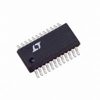
LTC4260IGN#PBF Linear Technology, LTC4260IGN#PBF Datasheet - Page 15

LTC4260IGN#PBF
Manufacturer Part Number
LTC4260IGN#PBF
Description
IC CTLR HOT SWAP I2C 24-SSOP
Manufacturer
Linear Technology
Type
Hot-Swap Controllerr
Datasheet
1.LTC4260CGNPBF.pdf
(28 pages)
Specifications of LTC4260IGN#PBF
Applications
General Purpose
Internal Switch(s)
No
Voltage - Supply
8.5 V ~ 80 V
Operating Temperature
-40°C ~ 85°C
Mounting Type
Surface Mount
Package / Case
24-SSOP (0.150", 3.90mm Width)
Family Name
LTC4260
Package Type
SSOP N
Operating Supply Voltage (min)
8.5V
Operating Supply Voltage (max)
80V
Operating Temperature (min)
-40C
Operating Temperature (max)
85C
Operating Temperature Classification
Industrial
Product Depth (mm)
3.99mm
Product Height (mm)
1.5mm
Mounting
Surface Mount
Pin Count
24
Lead Free Status / RoHS Status
Lead free / RoHS Compliant
Available stocks
Company
Part Number
Manufacturer
Quantity
Price
APPLICATIO S I FOR ATIO
Gate Pin Voltage
A curve of gate drive vs V
Performance curves. At the minimum input supply volt-
age of 8.5V, the minimum gate drive voltage is 4.5V.
When the input supply voltage is higher than 20V, the gate
drive is at least 10V and a regular N-FET can be used. In
applications over a 8.5V to 20V range, a logic level N-FET
must be used to maintain adequate gate enhancement.
The GATE pin is clamped at a typical value of 15V above
the SOURCE pin.
Configuring the GPIO Pin
Table 3 describes the possible states of the GPIO pin using
the control register bits A6 and A7. At power-up, the
default state is for the GPIO pin to go high impedance when
power is good (FB pin greater than 3.5V). Other uses for
the GPIO pin are to pull down when power is good, a
general purpose output and a general purpose input.
Compensating the Active Current Loop
The active current limit circuit is compensated using the
resistor R6 and the slew rate capacitor C1. The value for C1
is calculated to limit the inrush current. The suggested
value for R6 is 100k. This value should work for most pass
FETs (Q1). If the gate capacitance of Q1 is very small then
the best method to compensate the loop is to add a ≈10nF
capacitor between the GATE and SOURCE terminals.The
addition of 10Ω resistor (R5) prevents self-oscillation in
Q1 by isolating trace capacitance from the FETs GATE
Terminal. Locate the gate resistor at, or close to, the body
of the MOSFET.
Supply Transients
The LTC4260 is designed to ride through supply transients
caused by load steps. If there is a shorted load and the
parasitic inductance back to the supply is greater than
0.5µH, there is a chance that the supply could collapse
before the active current limit circuit brings down the
GATE pin. In this case the undervoltage monitors turn off
the pass FET. The undervoltage lockout circuit has a 5µs
filter time after V
in 2µs to shut the GATE off, but it is recommended to add
a filter capacitor C
by short transient. Eventually either the UV pin or the
DD
F
to prevent unwanted shutdown caused
U
drops below 7.5V. The UV pin reacts
U
DD
is shown in the Typical
W
U
undervoltage lockout responds to bring the current under
control before the supply completely collapses.
Supply Transient Protection
The LTC4260 is 100% tested and guaranteed to be safe
from damage with supply voltages up to 100V. However,
spikes above 100V may damage the part. During a short-
circuit condition, the large change in currents flowing
through the power supply traces can cause inductive
voltage spikes which could exceed 100V. To minimize the
spikes, the power trace inductance should be minimized
by using wider traces or heavier trace plating. Adding a
snubber circuit will dampen the voltage spikes. It is built
using a 100Ω resistor in series with a 0.1µF capacitor
between V
at the input will clamp the voltage spikes.
Design Example
As a design example, take the following specifications: V
= 48V, I
V
= 45V and I
sense resistor, R
50mV:
The FET should be sized to handle the power dissipation
during the inrush charging of the output capacitor C
The method used to determine the power is the principle:
Thus:
Calculate the time it takes to charge up C
The average power dissipated in the FET:
UVOFF
E
E
R
t
C
C
CHARGUP
S
= 1/2 CV
= Energy in C
=
= 38.5V, V
MAX
50
I
MAX
DD
mV
= 5A, I
2
and GND. A surge suppressor, Z1 in Figure 1,
C
=
2
ADDRESS
C
=
I
= 1/2(0.33mF)(48V)
INRUSH
OVOFF
S
L
, is set by the overcurrent threshold of
50
INRUSH
•
L
5
= Energy in Q1
V
mV
A
IN
= 70V, V
= 1010011. The selection of the
=
=
= 1A, C
330
0 010
.
PWRGDUP
µ
1
F
L
A
Ω
= 330µF, V
•
48
2
= 0.38J
V
LTC4260
= 46V, V
=
OUT
16
:
UVON
ms
PWRGDDN
15
= 43V,
OUT
4260fa
IN
.


