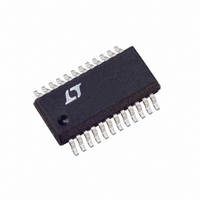
LTC4260IGN#PBF Linear Technology, LTC4260IGN#PBF Datasheet - Page 3

LTC4260IGN#PBF
Manufacturer Part Number
LTC4260IGN#PBF
Description
IC CTLR HOT SWAP I2C 24-SSOP
Manufacturer
Linear Technology
Type
Hot-Swap Controllerr
Datasheet
1.LTC4260CGNPBF.pdf
(28 pages)
Specifications of LTC4260IGN#PBF
Applications
General Purpose
Internal Switch(s)
No
Voltage - Supply
8.5 V ~ 80 V
Operating Temperature
-40°C ~ 85°C
Mounting Type
Surface Mount
Package / Case
24-SSOP (0.150", 3.90mm Width)
Family Name
LTC4260
Package Type
SSOP N
Operating Supply Voltage (min)
8.5V
Operating Supply Voltage (max)
80V
Operating Temperature (min)
-40C
Operating Temperature (max)
85C
Operating Temperature Classification
Industrial
Product Depth (mm)
3.99mm
Product Height (mm)
1.5mm
Mounting
Surface Mount
Pin Count
24
Lead Free Status / RoHS Status
Lead free / RoHS Compliant
Available stocks
Company
Part Number
Manufacturer
Quantity
Price
ELECTRICAL CHARACTERISTICS
temperature range, otherwise specifications are at T
SYMBOL
INTV
INTV
Gate Drive
t
∆V
I
I
I
I
Input Pins
V
∆V
I
V
∆V
I
V
∆V
I
V
∆V
∆V
I
V
∆V
I
V
∆V
I
V
∆V
V
I
R
I
Timer
V
V
I
I
I
D
GATE(UP)
GATE(FST)
GATE(DN)
SOURCE
ON(IN)
OV(IN)
UV(IN)
SENSE(IN)
FB
BD_PRST
GPIO(IN)
ADIN
TIMER(UP)
TIMER(DN)
TIMER(RATIO)
ON(TH)
OV(TH)
UV(TH)
UV(RTH)
FB
BD_PRST(TH)
GPIO(TH)
GPIO(OL)
TIMER(H)
TIMER(L)
ADIN
GATE
ON(HYST)
OV(HYST)
UV(HYST)
UV(RHYST)
SENSE(TH)
FB(HYST)
BD_PRST(HYST)
GPIO(HYST)
CC(UVL)
CC
PARAMETER
V
Internal Regulator Voltage
Turn-On Delay
External N-Channel Gate Drive
(V
External N-Channel Pull-Up Current
External N-Channel Fast Pull-Down
External N-Channel Pull-Down Current
SOURCE Pin Input Current
ON Pin Threshold Voltage
ON Pin Hysteresis
ON Pin Input Current
OV Pin Threshold Voltage
OV Pin Hysteresis
OV Pin Input Current
UV Pin Threshold Voltage
UV Pin Hysteresis
UV Pin Input Current
UV Pin Reset Threshold Voltage
UV Pin Reset Threshold Hysteresis
Current Limit Sense Voltage Threshold
(V
SENSE Pin Input Current
Foldback Pin Power Good Threshold
FB Pin Power Good Hysteresis
Foldback Pin Input Current
BD_PRST Input Threshold
BD_PRST Hysteresis
BD_PRST Pullup Current
GPIO Pin Input Threshold
GPIO Pin Hysteresis
GPIO Pin Output Low Voltage
GPIO Pin Input Leakage Current
ADIN Pin Input Resistance
ADIN Pin Input Current
TIMER Pin High Threshold
TIMER Pin Low Threshold
TIMER Pin Pull-Up Current
TIMER Pin Pull-Down Current
TIMER Pin Current Ratio
I
TIMER(DN)
CC
GATE
DD
Supply Undervoltage Lockout
– V
– V
SENSE
/I
SOURCE
TIMER(UP)
)
)
A
CONDITIONS
INTV
V
V
Gate Drive On, V
Fast Turn Off, V
Gate Drive Off, V
SOURCE = 48V
V
V
V
V
V
V
V
V
V
V
FB Rising
FB = 3.5V
V
BD_PRST = 0V
V
I
V
V
V
V
V
V
V
GPIO
= 25°C. V
DD
DD
ON
ON
OV
OV
UV
UV
UV
FB
FB
SENSE
BD_PRST
GPIO
GPIO
ADIN
ADIN
TIMER
TIMER
TIMER
TIMER
= 3.5V
= 0V
Rising
= 3.5V
Rising
= 3.5V
Falling
= 20V to 80V
= 8.5V to 20V
Rising
= 1.2V
CC
= 2mA
The
Rising
= 80V
= 1.28V
= 2.56V
= 48V
Rising
Falling
= 0V
= 1.3V
Falling
Rising
●
DD
denotes the specifications which apply over the full operating
= 48V, unless otherwise noted.
GATE
GATE
GATE
= 48V, V
= 0V
= 58V, V
SOURCE
SOURCE
= 38V
= 48V
●
●
●
●
●
●
●
●
●
●
●
●
●
●
●
●
●
●
●
●
●
●
●
●
●
●
●
●
●
●
●
●
●
●
●
●
●
●
●
1.19
3.43
3.43
1.18
3.43
MIN
–14
400
200
310
–80
3.4
4.5
0.7
1.2
1.6
1.2
0.1
1.4
1.6
50
10
60
70
80
45
10
70
80
70
–7
5
2
1.235
1.235
1.235
1.235
–100
0.25
TYP
–18
100
600
400
130
380
160
100
100
130
–10
3.8
5.5
3.5
3.5
3.5
1.8
0.2
14
90
50
20
80
10
6
1
0
0
0
0
0
0
2
2
LTC4260
MAX
1000
–120
1.27
3.56
3.56
1.27
3.56
1.27
1.28
150
–22
600
200
120
440
250
130
120
190
–16
±10
4.2
1.4
0.5
0.3
2.6
2.7
±1
18
18
±1
±1
±2
55
30
±2
6
2
UNITS
4260fa
3
MΩ
mA
mA
mV
mV
mV
mV
mV
mV
mV
mV
mV
ms
µA
µA
µA
µA
µA
µA
µA
µA
µA
µA
µA
µA
%
V
V
V
V
V
V
V
V
V
V
V
V
V
V


