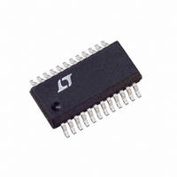
LTC4260IGN#PBF Linear Technology, LTC4260IGN#PBF Datasheet - Page 16

LTC4260IGN#PBF
Manufacturer Part Number
LTC4260IGN#PBF
Description
IC CTLR HOT SWAP I2C 24-SSOP
Manufacturer
Linear Technology
Type
Hot-Swap Controllerr
Datasheet
1.LTC4260CGNPBF.pdf
(28 pages)
Specifications of LTC4260IGN#PBF
Applications
General Purpose
Internal Switch(s)
No
Voltage - Supply
8.5 V ~ 80 V
Operating Temperature
-40°C ~ 85°C
Mounting Type
Surface Mount
Package / Case
24-SSOP (0.150", 3.90mm Width)
Family Name
LTC4260
Package Type
SSOP N
Operating Supply Voltage (min)
8.5V
Operating Supply Voltage (max)
80V
Operating Temperature (min)
-40C
Operating Temperature (max)
85C
Operating Temperature Classification
Industrial
Product Depth (mm)
3.99mm
Product Height (mm)
1.5mm
Mounting
Surface Mount
Pin Count
24
Lead Free Status / RoHS Status
Lead free / RoHS Compliant
Available stocks
Company
Part Number
Manufacturer
Quantity
Price
APPLICATIO S I FOR ATIO
LTC4260
The SOA (safe operating area) curves of candidate FETs
must be evaluated to ensure that the heat capacity of the
package can stand 24W for 16ms. The SOA curves of the
Fairchild FDB3632 provide for 1A at 50V (50W) for 10ms,
satisfying the requirement.
The inrush current is set to 1A using C1:
Default values of R5 = 10Ω and R6 = 100k are chosen as
discussed previously.
The power dissipated in the FET during overcurrent must
be limited. The active current limit uses a timer to prevent
excessive energy dissipation in the FET. The worst-case
power occurs when the voltage versus current profile of
the foldback current limit is at the maximum. This occurs
when the current is 5A and the voltage is 1/2 of the 48V or
24V. See the Current Limit Sense Voltage vs FB Voltage in
the Typical Performance curves to view this profile. In
order to survive 120W, the FET SOA curve dictates the
maximum time at this power level. This particular FET
allows 300W at 1ms or less. Therefore, it is acceptable to
set the current limit timeout using C
Note the minimum value for C
Choose R1, R2, R3, R7 and R8 for the UV, OV and PG
threshold voltages:
V
3.5V rising and 3.41V falling)
V
3.5V rising and 3.12V falling)
V
rising and 3.411V falling)
In addition a 0.1µF ceramic bypass capacitor is placed on
the INTV
16
OVRISING
UVRISING
PGRISING
P
C
C
DISS
1
T
=
=
C
CC
12
=
L
= 71.2V, V
= 46.14V, V
0 81
= 43V, V
I
pin. The complete circuit is shown in Figure 1.
t
GATE UP
I
[
.
CHARGUP
INRUSH
ms F
E
ms
/
(
C
µ
U
)
]
UVFALLING
OVFALLING
=
=
=
PGFALLING
0 33
68
0 38
16
.
U
nF
.
ms
mF
J
= 38.5V, (using V
T
= 69.44V (using V
≅
18
is 0.1nF.
= 45V, (using V
1
24
A
µ
W
A
W
T
to be 0.81ms:
=
5 9
.
nF
U
FB
UV(TH)
OV(TH)
= 3.5V
=
=
Layout Considerations
To achieve accurate current sensing, a Kelvin connection
is recommended. The minimum trace width for 1oz cop-
per foil is 0.02" per amp to make sure the trace stays at a
reasonable temperature. Using 0.03" per amp or wider is
recommended. Note that 1oz copper exhibits a sheet
resistance of about 530µΩ/ . Small resistances add up
quickly in high current applications. To improve noise
immunity, put the resistive divider to the UV, OV and FB
pins close to the device and keep traces to V
short. It is also important to put C3, the bypass capacitor
for the INTV
and GND. A 0.1µF capacitor from the UV pin (and OV pin
through resistor R2) to GND also helps reject supply
noise. Figure 5 shows a layout that addresses these
issues. Note that a surge suppressor, Z1, is placed be-
tween supply and ground using wide traces.
V
GND
IN
Z1
I
LOAD
C
F
CC
Figure 5. Recommended Layout for
R1, R2, R3, R8, C
R1
R2
R3
pin, as close as possible between INTV
SENSE RESISTOR R
F
, C3, Z1 and R
S
I
LOAD
SENSE
V
UV
OV
GND
DD
LTC4260
C3
S
INTV
DD
CC
FB
and GND
4260 F05
4260fa
CC
R
8


