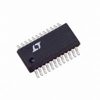
LTC4260IGN#PBF Linear Technology, LTC4260IGN#PBF Datasheet - Page 18

LTC4260IGN#PBF
Manufacturer Part Number
LTC4260IGN#PBF
Description
IC CTLR HOT SWAP I2C 24-SSOP
Manufacturer
Linear Technology
Type
Hot-Swap Controllerr
Datasheet
1.LTC4260CGNPBF.pdf
(28 pages)
Specifications of LTC4260IGN#PBF
Applications
General Purpose
Internal Switch(s)
No
Voltage - Supply
8.5 V ~ 80 V
Operating Temperature
-40°C ~ 85°C
Mounting Type
Surface Mount
Package / Case
24-SSOP (0.150", 3.90mm Width)
Family Name
LTC4260
Package Type
SSOP N
Operating Supply Voltage (min)
8.5V
Operating Supply Voltage (max)
80V
Operating Temperature (min)
-40C
Operating Temperature (max)
85C
Operating Temperature Classification
Industrial
Product Depth (mm)
3.99mm
Product Height (mm)
1.5mm
Mounting
Surface Mount
Pin Count
24
Lead Free Status / RoHS Status
Lead free / RoHS Compliant
Available stocks
Company
Part Number
Manufacturer
Quantity
Price
APPLICATIO S I FOR ATIO
LTC4260
address with the R/W bit now set to one. The LTC4260
acknowledges and sends the contents of the requested
register. The transmission is ended when the master
sends a STOP condition. If the master acknowledges the
transmitted data byte, as in a Read Word command
(Figure 12), the LTC4260 will repeat the requested register
as the second data byte.
Note that the Register Address pointer is not cleared at the
end of the transaction. Thus the Receive Byte protocol can
be used to repeatedly read a specific register.
Alert Response Protocol
The LTC4260 implements the SMBus Alert Response
Protocol as shown in Figure 11. If enabled to do so through
the ALERT register B, the LTC4260 will respond to faults
by pulling the ALERT pin low. Multiple LTC4260s can
share a common ALERT line and the protocol allows a
master to determine which LTC4260s are pulling the line
18
SDA
SCL
CONDITION
START
S
U
U
ADDRESS
a6 - a0
1 - 7
W
R/W
8
Figure 6. Data Transfer Over I
ACK
9
U
1 - 7
b7 - b0
DATA
low. The master begins by sending a START bit followed
by the special Alert Response Address (0001 100)b with
the R/W bit set to one. Any LTC4260 that is pulling its
ALERT pin low will acknowledge and begin sending back
its individual slave address.
An arbitration scheme ensures that the LTC4260 with the
lowest address will have priority; all others will abort their
response. The successful responder will then release its
ALERT pin while any others will continue to hold their
ALERT pins low. Polling may also be used to search for any
LTC4260 that have detected faults. Any LTC4260 pulling
its ALERT pin low will also release it if it is individually
addressed during a read or write transaction.
The ALERT signal will not be pulled low again until the
FAULT register indicates a different fault has occurred or
the original fault is cleared and it occurs again. Note that
this means repeated or continuing faults will not generate
alerts until the associated FAULT register bit has been
cleared.
8
2
C or SMBus
ACK
9
1 - 7
b7 - b0
DATA
8
ACK
9
CONDITION
STOP
P
4260 F06
4260fa


