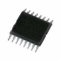
PCA9551PW,112 NXP Semiconductors, PCA9551PW,112 Datasheet - Page 12

PCA9551PW,112
Manufacturer Part Number
PCA9551PW,112
Description
IC LED DRIVER BLINKER 16-TSSOP
Manufacturer
NXP Semiconductors
Type
LED Blinkerr
Datasheet
1.PCA9551BS118.pdf
(26 pages)
Specifications of PCA9551PW,112
Package / Case
16-TSSOP
Topology
Open Drain, PWM
Number Of Outputs
8
Internal Driver
Yes
Type - Primary
LED Blinker
Frequency
400kHz
Voltage - Supply
2.3 V ~ 5.5 V
Mounting Type
Surface Mount
Operating Temperature
-40°C ~ 85°C
Current - Output / Channel
25mA
Internal Switch(s)
Yes
Low Level Output Current
6.5 mA
Operating Supply Voltage
2.3 V to 5.5 V
Maximum Power Dissipation
400 mW
Maximum Operating Temperature
+ 85 C
Mounting Style
SMD/SMT
Minimum Operating Temperature
- 40 C
Lead Free Status / RoHS Status
Lead free / RoHS Compliant
For Use With
OM6285 - EVAL BOARD I2C-2002-1A568-4002 - DEMO BOARD I2C568-3615 - DEMO BOARD I2C
Voltage - Output
-
Efficiency
-
Lead Free Status / Rohs Status
Lead free / RoHS Compliant
Other names
568-1048-5
935271692112
PCA9551PW
935271692112
PCA9551PW
NXP Semiconductors
9. Limiting values
PCA9551_8
Product data sheet
8.2 Programming example
The following example will show how to set LED0 to LED3 on. It will then set LED4 and
LED5 to blink at 1 Hz at a 50 % duty cycle. LED6 and LED7 will be set to blink at 4 Hz and
at a 25 % duty cycle.
Table 10.
Table 11.
In accordance with the Absolute Maximum Rating System (IEC 60134).
Program sequence
START
PCA9551 address with A0 to A2 = LOW
PSC0 subaddress + Auto-Increment
Set prescaler PSC0 to achieve a period of 1 second:
PSC0 = 37
Set PWM0 duty cycle to 50 %:
PWM0 = 128
Set prescaler PSC1 to achieve a period of 0.25 seconds:
PSC1 = 9
Set PWM1 output duty cycle to 25 %:
PWM1 = 192
Set LED0 to LED3 on
Set LED4 and LED5 to PWM0, and LED6 or LED7 to PWM1
STOP
Symbol
V
V
I
I
P
T
T
O(LEDn)
SS
stg
amb
DD
I/O
tot
Blink period
256 PWM0
--------------------------------
Blink period
256 PWM1
--------------------------------
–
–
256
256
Programming PCA9551
Limiting values
Parameter
supply voltage
voltage on an input/output pin
output current on pin LEDn
ground supply current
total power dissipation
storage temperature
ambient temperature
=
=
=
=
0.5
0.25
1
0.25
=
PSC0
----------------------- -
=
Rev. 08 — 31 July 2008
PSC1
----------------------- -
38
+
38
1
+
8-bit I
1
2
C-bus LED driver with programmable blink rates
Conditions
operating
Min
V
-
-
-
0.5
65
40
SS
0.5
PCA9551
© NXP B.V. 2008. All rights reserved.
Max
+6.0
5.5
100
400
+150
+85
I
S
C0h
11h
25h
80h
09h
C0h
00h
FAh
P
25
2
C-bus
12 of 26
Unit
V
V
mA
mA
mW
C
C


