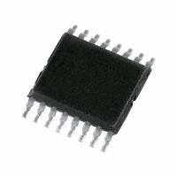
PCA9551PW,112 NXP Semiconductors, PCA9551PW,112 Datasheet - Page 6

PCA9551PW,112
Manufacturer Part Number
PCA9551PW,112
Description
IC LED DRIVER BLINKER 16-TSSOP
Manufacturer
NXP Semiconductors
Type
LED Blinkerr
Datasheet
1.PCA9551BS118.pdf
(26 pages)
Specifications of PCA9551PW,112
Package / Case
16-TSSOP
Topology
Open Drain, PWM
Number Of Outputs
8
Internal Driver
Yes
Type - Primary
LED Blinker
Frequency
400kHz
Voltage - Supply
2.3 V ~ 5.5 V
Mounting Type
Surface Mount
Operating Temperature
-40°C ~ 85°C
Current - Output / Channel
25mA
Internal Switch(s)
Yes
Low Level Output Current
6.5 mA
Operating Supply Voltage
2.3 V to 5.5 V
Maximum Power Dissipation
400 mW
Maximum Operating Temperature
+ 85 C
Mounting Style
SMD/SMT
Minimum Operating Temperature
- 40 C
Lead Free Status / RoHS Status
Lead free / RoHS Compliant
For Use With
OM6285 - EVAL BOARD I2C-2002-1A568-4002 - DEMO BOARD I2C568-3615 - DEMO BOARD I2C
Voltage - Output
-
Efficiency
-
Lead Free Status / Rohs Status
Lead free / RoHS Compliant
Other names
568-1048-5
935271692112
PCA9551PW
935271692112
PCA9551PW
NXP Semiconductors
PCA9551_8
Product data sheet
6.3.3 PWM0 - Pulse Width Modulation 0
6.3.4 PSC1 - Frequency Prescaler 1
6.3.5 PWM1 - Pulse Width Modulation 1
Table 5.
The PWM0 register determines the duty cycle of BLINK0. The outputs are LOW (LED off)
when the count is less than the value in PWM0 and HIGH when it is greater. If PWM0 is
programmed with 00h, then the PWM0 output is always LOW.
The duty cycle of BLINK0 = (256
Table 6.
PSC1 is used to program the period of the PWM output.
The period of BLINK1 = (PSC1 + 1) / 38.
Remark: Prescaler calculation is different between the PCA9551 and other PCA955x
LED blinkers. A divider ratio of 38 instead of 44 is used. This different divider ratio causes
the blinking frequency to be 13 % (1
The programmed value of Frequency Prescaler 1 must be adjusted to compensate for this
difference in applications where the PCA9551 is used in conjunction with other PCA955x
LED blinkers and the observed blinking frequencies need to be the same.
Table 7.
The PWM1 register determines the duty cycle of BLINK1. The outputs are LOW (LED off)
when the count is less than the value in PWM1 and HIGH when it is greater. If PWM1 is
programmed with 00h, then the PWM1 output is always LOW (LED off).
The duty cycle of BLINK1 = (256
Table 8.
Bit
Symbol
Default
Bit
Symbol
Default
Bit
Symbol
Default
Bit
Symbol
Default
PSC0 - Frequency Prescaler 0 register description
PSC0[7]
PWM0 - Pulse Width Modulation 0 register description
PSC1 - Frequency Prescaler 1 register description
PSC1[7]
PWM1 - Pulse Width Modulation 1 register description
PWM0
PWM1
[7]
[7]
7
1
7
1
7
1
7
1
PSC0[6]
PSC1[6]
PWM0
PWM1
[6]
[6]
Rev. 08 — 31 July 2008
6
1
6
0
6
1
6
0
8-bit I
PSC0[5]
PSC1[5]
PWM0
PWM1
[5]
[5]
5
1
5
0
5
1
5
0
PWM0) / 256.
PWM1) / 256.
2
C-bus LED driver with programmable blink rates
38 / 44) lower when the same 8-bit word is used.
PSC0[4]
PSC1[4]
PWM0
PWM1
[4]
[4]
4
1
4
0
4
1
4
0
PSC0[3]
PSC1[3]
PWM0
PWM1
[3]
[3]
3
1
3
0
3
1
3
0
PSC0[2]
PSC1[2]
PWM0
PWM1
[2]
[2]
2
2
0
2
2
0
1
1
PCA9551
PSC0[1]
PSC1[1]
© NXP B.V. 2008. All rights reserved.
PWM0
PWM1
[1]
[1]
1
1
1
0
1
1
1
0
PSC0[0]
PSC1[0]
PWM0
PWM1
[0]
[0]
0
1
0
0
0
1
0
0
6 of 26


