LP5520TL/NOPB National Semiconductor, LP5520TL/NOPB Datasheet
LP5520TL/NOPB
Specifications of LP5520TL/NOPB


Related parts for LP5520TL/NOPB


LP5520TL/NOPB Summary of contents
Page 1
... Temperature is measured using an external temperature sen- sor placed close to the LEDs. The second ADC input can be used e.g. for ambient light measurement. LP5520 is available in 25 pin microSMD™ package. Typical Application © 2007 National Semiconductor Corporation Features ■ Temperature compensated LED intensity and color ■ ...
Page 2
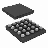
Connection Diagrams Thin microSMD-25 Package, Large Bump NS Package Number TLA25EMA 2.77 x 2.59 × 0.6 mm Top View Ordering Information Order Number LP5520TL LP5520TLX www.national.com 20186108 Package Mark – Top View Package Marking Supplied As 5520 250 units, Tape-and-Reel ...
Page 3
Pin Descriptions Pin Name Type 5E SW Output 5D FB Input 5C VDDD Power 5B SI/A0 Logic Input 5A SO Logic Output 4E GND_SW Ground 4D PWMR Logic Input 4C IFSEL Logic Input 4B SCK/SCL Logic Input 4A SS/SDA Logic ...
Page 4
... J Note 4: For detailed soldering specifications and information, please refer to National Semiconductor Application Note AN1112 : MicroSMD Wafer Level Chip Scale Package Note 5: The Human body model is a 100 pF capacitor discharged through a 1.5 kΩ resistor into each pin. The machine model is a 200 pF capacitor discharged directly into each pin ...
Page 5
Block Diagram Modes of Operation LP5520 has three different operating modes: Manual mode, Automatic mode and Stand-Alone mode. The Automatic mode has two sub modes, normal mode and sequential mode. In manual and automatic modes the chip is controlled <RGB_auto> ...
Page 6
EEPROM. This EEP- ROM address is then used to get the PWM values for each output. The second input S2_IN can be used for example for ambient light measurement. The ADC data from selected ...
Page 7
LP5520 control and output waveforms in stand-alone mode Start-Up START-UP POWERING V and V should be tied together and turned on first. DDD DDA V must be turned on at the same time as V DDIO LP5520 connection in stand-alone ...
Page 8
START-UP SEQUENCE RESET: In the RESET mode all the internal registers are reset to the default values and the chip goes to STANDBY mode after reset. <NSTBY> control bit is low after reset by default. Reset is entered always if ...
Page 9
RGB Driver Functionality WHITE BALANCE CONTROL LP5520 is designed to provide spectrally rich white light using a three color RGB LED. White light is obtained when the Red, Green and Blue LED intensities are in proper balance. The LED intensities ...
Page 10
Compensated Color Coordinates vs. Temperature CALIBRATION MEMORY The 1 kbit calibration EEPROM memory is organized as 128 x 8 bits. It stores the 12-bit calibration PWM values for each output at 16°C intervals. 10 temperature points are used to cover ...
Page 11
EEPROM memory map Address Bits [7:4] 00 RB0[7:0] 01 RB1[7:0] 02 RB2[7:0] 03 RB3[7:0] 04 RB4[7:0] 05 RB5[7:0] 06 RB6[7:0] 07 RB7[7:0] 08 RB8[7:0] 09 RB9[7:0] 0a GB0[7:0] 0b GB1[7:0] 0c GB2[7:0] 0d GB3[7:0] 0e GB4[7:0] 0f GB5[7:0] 10 GB6[7:0] ...
Page 12
Address Bits [7:4] 4a GC0[7:0] 4b GC1[7:0] 4c GC2[7:0] 4d GC3[7:0] 4e GC4[7:0] 4f GC5[7:0] 50 GC6[7:0] 51 GC7[7:0] 52 GC8[7:0] 53 GC9[7:0] 54 BC0[7:0] 55 BC1[7:0] 56 BC2[7:0] 57 BC3[7:0] 58 BC4[7:0] 59 BC5[7:0] 5a BC6[7:0] 5b BC7[7:0] 5c ...
Page 13
The EEPROM data can be read, written and erased through the serial interface. The boost converter is used to generate the write and erase voltage for the memory. All operations are done in page mode. The page address has to ...
Page 14
LED BRIGHTNESS CONTROL The LED brightness is defined by two factors, the current through the LED and the PWM duty cycle. The constant cur- rent outputs ROUT, GOUT and BOUT can be independently set to sink between 0 and 60 ...
Page 15
SEQUENTIAL MODE Completely non-overlapping timing can be obtained by using the sequential mode as shown in the graph below. The timing is defined with external PWM control inputs. The minimum Non-overlapping external synchronized sequential mode In sequential mode the PWM ...
Page 16
PWM mode defined by <seq_mode1> and <seq_mode2> control bits of rgb_control (00H) register: <seq_mode1> (bit CURRENT CONTROL OF THE LEDS LP5520 has separate 8-bit current control for each LED out- put. In manual mode the ...
Page 17
RGB DRIVER ELECTRICAL CHARACTERISTICS (R Symbol Parameter and B pin LEAKAGE OUT OUT OUT leakage current I Maximum Sink Current MAX I Current accuracy OUT G and B OUT OUT I Matching ...
Page 18
Temperature and Light Measurement LP5520 has a 12-bit Analog-to-Digital Converter for the mea- surements. The ADC has two inputs. S1_IN input is intended for the LM20 temperature sensor and S2_IN input for light measurement or any DC voltage measurement. The ...
Page 19
Magnetic High Voltage Boost DC/DC Converter The LP5520 Boost DC/DC Converter generates 20V supply voltage for the LEDs from single Li-Ion battery (2.9 to 4.5V). The output voltage is controlled with four bits in 18 steps. In ...
Page 20
MAGNETIC BOOST DC/DC CONVERTER ELECTRICAL CHARACTERISTICS Symbol Parameter I Maximum LOAD Continuous Load Current V Output Voltage OUT Accuracy (FB Pin) RDS Switch ON ON Resistance f Frequency PWM Accuracy t Switch Pulse PULSE Minimum Width t Startup Time STARTUP ...
Page 21
Boost Converter Typical Performance Characteristics V = 3.6V 15.0V if not otherwise stated IN OUT Boost Converter Efficiency Boost Max. Output Voltage vs. Current Autoload Effect on Input Current, No Load Boost Typical Waveforms Load ...
Page 22
Logic Interface Characteristics Symbol Parameter Logic Inputs SS, SI/A0, SCK/SCL, IFSEL, NRST, PWMR, PWMG, PWMB and BRC V Input Low Level IL V Input High Level IH I Logic Input Current I I SPI Mode f V Clock Frequency SCK/SLC ...
Page 23
SPI TIMING PARAMETERS 2.775V DDA DDD DD_IO Symbol Parameter 1 Cycle Time 2 Enable Lead Time 3 Enable Lag Time 4 Clock Low Time 5 Clock High Time 6 Data Setup Time 7 Data ...
Page 24
Compatible Interface SIGNALS The serial interface mode when IF_SEL = 0. The SCL pin is used for the clock and the SDA pin is used for ...
Page 25
When a READ function accomplished, a WRITE func- tion must precede the READ function, as shown in the I Read Cycle waveform TIMING PARAMETERS (V = 3.0 to 4.5V, V DD1,2 Symbol 1 Hold ...
Page 26
Recommended External Components OUTPUT CAPACITOR: C OUT The output capacitor C directly affects the magnitude of OUT the output ripple voltage. In general, the higher the value the lower the output ripple magnitude. Multilayer ce- OUT ramic ...
Page 27
LP5520 Registers, Control Bits and Default Values All registers will have their default value after power-on or reset. Default value for correction registers is 1000 0000 (multiplier = 1). Default value for adaptive voltage control and fast PWM is on. ...
Page 28
REGISTER BIT CONVENTIONS Each register is shown with a key indicating the accessibility of the each individual bit, and the initial condition: Register Bit Accessibility and Initial Condition rgb_control (00H) – RGB LEDs Control Register 7 6 seq_mode1 seq_mode0 rw-0 ...
Page 29
Green LED Current Control Register 7 6 cc_g[7] cc_g[6] rw-0 rw-1 current_control_B (03H) – Blue LED Current Control Register 7 6 cc_b[7] cc_b[6] rw-0 rw-1 pwm_brightness (04H) – Brightness Control Register 7 6 r-0 r-0 Bit 4 ...
Page 30
Boost Output Voltage Control Register 7 6 r-0 r-0 Bits vprog[4:0] control (06H) – Control Register adc_ch r-0 r-0 rw-0 adc_ch comp_sel en_autoload vout_auto en_boost nstby ADC_hi_byte (08H) – Analog Digital ...
Page 31
ADC_low_byte (09H) – Analog Digital Converter Output, bits 0 adc[7] adc[6] r-0 r-0 r_correction (0AH) – Additional Brightness Correction Value Register for Red LED 7 6 corr_r[7] corr_r[6] corr_r[5] rw-1 rw-0 corr_r[7:0] g_correction (0BH) – Additional Brightness Correction ...
Page 32
Physical Dimensions The dimension for X1 ,X2 and X3 are as given: — 2.77 mm ± 0.03 mm — 2.59 mm ± 0.03 mm — 0.6 mm ± 0.075 mm www.national.com inches (millimeters) unless ...
Page 33
Notes 33 www.national.com ...
Page 34
... National Semiconductor and the National Semiconductor logo are registered trademarks of National Semiconductor Corporation. All other brand or product names may be trademarks or registered trademarks of their respective holders. ...