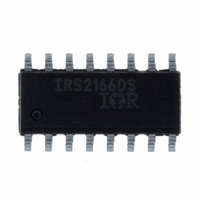
IRS2166DSPBF International Rectifier, IRS2166DSPBF Datasheet - Page 10

IRS2166DSPBF
Manufacturer Part Number
IRS2166DSPBF
Description
IC PFC/BALLAST/HALF BRDG 16-SOIC
Manufacturer
International Rectifier
Type
PFC/Ballast Controllerr
Datasheet
1.IRS2166DSPBF.pdf
(18 pages)
Specifications of IRS2166DSPBF
Frequency
40 ~ 46 kHz
Current - Supply
20mA
Current - Output
260mA
Voltage - Supply
12.5 V ~ 15.6 V
Operating Temperature
-25°C ~ 125°C
Package / Case
16-SOIC (3.9mm Width)
For Use With
IRPLLNR7 - KIT UNIV ELEC BALLAST FLUOR LAMP
Lead Free Status / RoHS Status
Lead free / RoHS Compliant
Available stocks
Company
Part Number
Manufacturer
Quantity
Price
Company:
Part Number:
IRS2166DSPBF
Manufacturer:
IR
Quantity:
9 182
www.irf.com
gate of a p-channel MOSFET (S4) (see Fig. 4) that
connects pin RPH with pin RT. As pin CPH exceeds 10.8
V (V
begins to fall below the turn-on threshold of S4. As pin
CPH continues to ramp towards V
slowly. This results in resistor R
smoothly from resistor R
frequency to ramp smoothly from the preheat frequency,
through the ignition frequency, to the final run frequency.
The over-current threshold on pin CS will protect the
ballast against a non-strike or open-filament lamp fault
condition. The voltage on pin CS is defined by the lower
half-bridge MOSFET current flowing through the external
current sensing resistor R
programs the maximum allowable peak ignition current
(and therefore peak ignition voltage) of the ballast output
stage. The peak ignition current must not exceed the
maximum allowable current ratings of the output stage
MOSFETs. Should this voltage exceed the internal
threshold of 1.20 V (V
begins counting the number of of sequential over-current
faults (see timing diagram). If the number of over-current
faults exceeds 50 (n
and gate driver outputs HO, LO and PFC will be latched
low.
Run Mode (RUN)
Once the lamp has successfully ignited, the ballast enters
run mode. The run mode is defined as the state the IC is
in when the lamp arc is established and the lamp is being
driven to a given power level. The run mode oscillating
frequency is determined by the timing resistor R
timing capacitor C
Should hard-switching occur at the half-bridge at any time
due to an open-filament or lamp removal, the voltage
across the current sensing resistor, R
internal threshold of 1.20 V (V
will begin counting (see timing diagram).
number of consecutive over-current faults exceed 50
(n
outputs HO, LO and PFC will be latched low.
EVENTS
CPHEOP
V
V
BUS
BUS
), the IC will enter fault mode and gate driver
(+)
(-)
), the gate-to-source voltage of MOSFET S4
C
R
R
C
CPH
T
PH
T
CPH
RPH
R
T
C
T
3
4
5
2
Fig. 3: Preheat circuitry
S4
T
EVENTS
5uA
(see Design Equations, page 15).
CSTH+
), the IC will enter FAULT mode
T
OSC.
, which causes the operating
CS
. The resistor R
), the internal fault counter
CSTH+
IRS2166D
Bridge
Driver
Half-
PH
CC
) and the fault counter
, switch S4 turns off
being disconnected
16
15
11
12
CS
HO
VS
LO
COM
, will exceed the
CS
Should the
M1
M2
RCS
Bridge
Output
Load
Return
Half-
I
therefore
LOAD
T
and
DC Bus Undervoltage Reset
Should the DC bus decrease too low during a brown-out
line condition or over-load condition, the resonant output
stage to the lamp can shift near or below resonance. This
can produce hard-switching at the half-bridge which can
damage the half-bridge switches or, the DC bus can
decrease too far and the lamp can extinguish. To protect
against this, the VBUS pin includes a 3.0 V undervoltage
threshold (V
decrease below 3.0 V, V
V
low.
For proper ballast design, the designer should design the
PFC section such that the DC bus does not drop until the
AC line input voltage falls below the rated input voltage of
the ballast (see PFC section). When correctly designed,
the voltage measured at the VBUS pin will decrease
below the internal 3.0 V threshold (VBUSUV) and the
ballast will turn off cleanly. The pull-up resistor to V
(R
input line voltage increases to the minimum specified
value causing V
R
minimum specified ballast input voltage. The PFC should
then be designed such that the DC bus decreases at an
input line voltage that is lower than the minimum specified
ballast input voltage. This hysteresis will result in clean
turn-on and turn-off of the ballast.
SD/EOL and CS Fault Mode (FAULT)
Should the voltage at the SD/EOL pin exceed 3.0 V
(V
mode, an end-of-life (EOL) fault condition has occurred
and the IC enters fault mode. LO, HO, and PFC gate
driver outputs are all latched off in the ‘low’ state. C
discharged to COM for resetting the preheat time. To exit
fault mode, V
power off) or the SD pin can be increased above 5.0 V
(V
to enter UVLO mode (see State Diagram, page 7). Once
CCUV
SUPPLY
EOLTH+
SDTH+
SUPPLY
- threshold and all gate driver outputs will be latched
V
V
BUS
BUS
) (lamp removal). Either of these will force the IC
) or decrease below 1.0 V (V
) will then turn the ballast on again when the AC
(+)
(-)
should be set to turn the ballast on at the
C
R
R
C
CPH
BUSUV
T
PH
T
CC
CPH
VCC
RPH
CT
RT
CC
can be decreased below V
13
3
4
5
2
). Should the voltage at the VBUS pin
Fig.4: Ignition circuitry
to exceed V
S
S
4
5uA
1
S
3
CC
OSC
Fault
Logic
IRS2166D(S)PbF
will be discharged below the
Comp 4
CCUV
IRS2166D
Bridge
Driver
Half-
1.3V
+.
16
15
11
10
12
HO
EOLTH-
VS
LO
CS
COM
C
CS
R1
CCUV
) during run
M1
M2
R
Bridge
Output
CS
Load
Return
Half-
I
LOAD
- (ballast
PH
CC
is
Page 10


