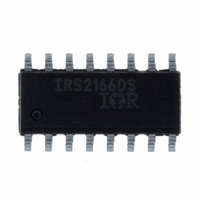
IRS2166DSPBF International Rectifier, IRS2166DSPBF Datasheet - Page 14

IRS2166DSPBF
Manufacturer Part Number
IRS2166DSPBF
Description
IC PFC/BALLAST/HALF BRDG 16-SOIC
Manufacturer
International Rectifier
Type
PFC/Ballast Controllerr
Datasheet
1.IRS2166DSPBF.pdf
(18 pages)
Specifications of IRS2166DSPBF
Frequency
40 ~ 46 kHz
Current - Supply
20mA
Current - Output
260mA
Voltage - Supply
12.5 V ~ 15.6 V
Operating Temperature
-25°C ~ 125°C
Package / Case
16-SOIC (3.9mm Width)
For Use With
IRPLLNR7 - KIT UNIV ELEC BALLAST FLUOR LAMP
Lead Free Status / RoHS Status
Lead free / RoHS Compliant
Available stocks
Company
Part Number
Manufacturer
Quantity
Price
Company:
Part Number:
IRS2166DSPBF
Manufacturer:
IR
Quantity:
9 182
www.irf.com
Should high currents occur, the voltage across the current-
sensing resistor will exceed 4.3V over-voltage protection
threshold at the VBUS pin and the PFC MOSFET will turn off
safely limiting the current. The watch-dog timer will then restart
the PFC as normal (Fig. 15). The current sensing resistor
value should be selected such that the over-current protection
does not false trip during normal operation over the entire line
voltage and load range. A current-sensing resistor value of 1.0
ohm, for example, will set the over-current threshold to about 5
A peak.
The effect that these line and load conditions have on the
performance of the ballast depends on the saturation level of
the PFC inductor, the selection of the PFC MOSFET, the DC
bus capacitor value, the maximum on-time limit set by the
DZCOMP, and, how fast VCC decreases below UVLO-.
protection circuit (upper trace: DC Bus, 100V/div; middle trace:
Rect (+)
Rect (-)
AC line input voltage, 100V/div; lower trace: PFC inductor
Fig. 15: PFC inductor current limited using over-current
Fig. 14: External over-current protection circuit
LPFC
MPFC
RS
1
DPFC
CBUS
current 1A/div).
47
RD
1N4148
DOC
COMP
VBUS
CPH
RPH
PFC
RT
CT
ZX
DC Bus
1
2
3
4
5
7
6
7
8
16
15
14
13
12
11
10
9
COM
HO
VS
VB
VCC
LO
CS
SD/ EOL
For these reasons, the ballast designer should perform
these mains interrupt and ignition tests carefully to
determine the correct current-sensing resistor value and
determine the robustness of their final design.
Ballast Design Equations
Note: The results from the following design equations can
differ slightly from experimental measurements due to IC
tolerances, component tolerances, and oscillator over-
and under-shoot due to internal comparator response
time.
Step 1: Program Deadtime
The deadtime between the gate driver outputs HO and
LO is programmed with timing capacitor C
internal deadtime resistor R
discharge time of capacitor C
and is given as:
or
Step 2: Program Run Frequency
The final run frequency is programmed with timing
resistor R
capacitor C
time of HO and LO gate driver outputs. The run frequency
is therefore given as:
or
Step 3: Program Preheat Frequency
The preheat frequency is programmed with timing
resistors R
resistors are connected in parallel internally for the
duration of the preheat time. The preheat frequency is
therefore given as:
f
RUN
t
C =
R
DT
T
T
T
=
=
=
T
T
and timing capacitor C
and R
2
C
. 1
1475
from 1/3 V
t
⋅
T
DT
02
C
⋅
1475
T
PH
⋅
(
C
, and timing capacitor C
. 0
1
T
51
CC
⋅
IRS2166D(S)PbF
1
⋅
f
to 3/5 V
RUN
R
T
DT
T
+
. The deadtime is the
from 3/5 V
−
1475
T
2892
CC
. The charge time of
determines the on-
)
CC
T
[Hz]
. The timing
[Ω]
to 1/3 V
[s]
[F]
T
and an
(1)
(2)
(4)
(3)
CC
Page 14


