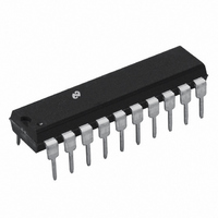
LMD18400N/NOPB National Semiconductor, LMD18400N/NOPB Datasheet - Page 11

LMD18400N/NOPB
Manufacturer Part Number
LMD18400N/NOPB
Description
IC DRIVER QUAD HI SIDE 20-DIP
Manufacturer
National Semiconductor
Datasheet
1.LMD18400NNOPB.pdf
(19 pages)
Specifications of LMD18400N/NOPB
Configuration
High-Side
Input Type
Non-Inverting
Delay Time
5µs
Current - Peak
3A
Number Of Configurations
4
Number Of Outputs
4
Voltage - Supply
7 V ~ 28 V
Operating Temperature
-25°C ~ 85°C
Mounting Type
Through Hole
Package / Case
20-DIP (0.300", 7.62mm)
Supply Voltage Min
7V
Supply Voltage Max
60V
No. Of Outputs
4
Output Voltage
5.5V
Output Current
3.75A
Driver Case Style
DIP
Msl
MSL 1 - Unlimited
Device Type
High Side
Rohs Compliant
Yes
Lead Free Status / RoHS Status
Lead free / RoHS Compliant
High Side Voltage - Max (bootstrap)
-
Other names
*LMD18400N
*LMD18400N/NOPB
LMD18400N
*LMD18400N/NOPB
LMD18400N
Available stocks
Company
Part Number
Manufacturer
Quantity
Price
Company:
Part Number:
LMD18400N/NOPB
Manufacturer:
National Semiconductor
Quantity:
135
Applications Information
Thermal Protection
The die temperature of the LMD18400 is continually moni-
tored. Should any conditions cause the die temperature to
rise to +170˚C, all of the power switches are turned OFF
automatically to reduce the power dissipation. It is important
to realize that the thermal shutdown affects all four of the
switches together. That is, if just one switch load is enough to
heat the die to the thermal shutdown threshold, all of the
other switches, regardless of their power dissipation condi-
tions, will be switched OFF. All of the switches will be re-
enabled when the die temperature has cooled to approxi-
mately +160˚C. Until the high temperature forcing conditions
have been removed the switches will cycle ON and OFF thus
maintaining an average die temperature of +165˚C. The
LMD18400 will signal that excessive temperatures exist
through several diagnostic output signals (see Diagnostics).
DIAGNOSTICS
The LMD18400 has extensive circuit diagnostic information
reporting capability. Use of this information can produce
systems with intelligent feedback of switch status as well as
load fault conditions for troubleshooting purposes. All of the
diagnostic information is contained in an 11-bit word. This
data can be clocked out of the LMD18400 in a serial fashion
as shown in Figure 8. The shift register is parallel loaded with
the diagnostic data whenever the Chip Select input is at a
Logic 1 and changes to the serial shift mode when Chip
Select is taken to a Logic 0. The Data Output line (pin 8) is
FIGURE 7. Driving a Large Capacitive Load
Capacitive Load
Driving a Large
(Continued)
01102616
11
biased internally from a 5.1V regulator which sets the Logic
1 output voltage. This pin has low current sourcing capability
so any load on this pin will reduce the Logic 1 output level
which is guaranteed to be at least 2.4V with a 360 µA load.
The data interface is MICROWIRE compatible in that data is
clocked out of the LMD18400 on the falling edge of the clock,
to be clocked into the controlling microprocessor on the
rising edge. Any number of devices can share a common
data output line because the data output pin is held in a high
impedance (TRI-STATE) condition until the device is se-
lected by taking its Chip Select Input low. Following Chip
Select going low there is a short data setup time interval
(500 ns Min) required. This is necessary to allow the first
data bit of information to be established on the data output
line prior to the first rising clock edge which will input the data
bit into the controller. When all 11 bits of diagnostic data
have been shifted out the data output goes to a Logic 1 level
until the Chip Select line is returned high.
Figure 8 also indicates the significance of the diagnostic data
bits. The first 4 bits indicate an output load error condition,
one for each channel in succession (see Load Error Detec-
tion).
Bits 5 through 8 provide a readback of the commanded
ON/OFF status of each switch.
A unique feature of the LMD18400 is that it provides an early
warning of excessive operating temperature. Should the die
temperature exceed +145˚C, bit 9 will be set to a Logic 0.
Acting on this information a system can be programmed to
take corrective action, shutting OFF specific loads perhaps,
while the LMD18400 is still operating normally (not yet in
thermal shutdown). If this early warning is ignored and the
device continues to rise in temperature, the thermal shut-
down circuitry will come into action at a die temperature of
+170˚C. Should this occur bit 10 of the diagnostic data
stream will be set to a Logic 0 indicating that the device is in
thermal shutdown and all of the outputs have been shut OFF.
The final data bit, bit 11, indicates an overvoltage condition
on the V
indicates that all of the drivers are OFF.
The diagnostic data can be read periodically by a controller
or only in the event of a general system error indication to
determine the cause of any system problem. This general
indication of a fault is provided by an Error Flag output (pin
13). This pin goes low whenever any type of error is de-
tected. There is a built-in delay of approximately 75 µs from
the time an error is detected until pin 13 is taken low. This is
to help mask short duration error conditions such as may be
caused by driving highly capacitive loads (
load may generate a shorted load error for several hundred
milliseconds as it turns on which should be ignored.
CC
supply (V
CC
is greater than 35V) and again
>
2 µF). A lamp
www.national.com


