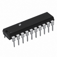
LMD18400N/NOPB National Semiconductor, LMD18400N/NOPB Datasheet - Page 8

LMD18400N/NOPB
Manufacturer Part Number
LMD18400N/NOPB
Description
IC DRIVER QUAD HI SIDE 20-DIP
Manufacturer
National Semiconductor
Datasheet
1.LMD18400NNOPB.pdf
(19 pages)
Specifications of LMD18400N/NOPB
Configuration
High-Side
Input Type
Non-Inverting
Delay Time
5µs
Current - Peak
3A
Number Of Configurations
4
Number Of Outputs
4
Voltage - Supply
7 V ~ 28 V
Operating Temperature
-25°C ~ 85°C
Mounting Type
Through Hole
Package / Case
20-DIP (0.300", 7.62mm)
Supply Voltage Min
7V
Supply Voltage Max
60V
No. Of Outputs
4
Output Voltage
5.5V
Output Current
3.75A
Driver Case Style
DIP
Msl
MSL 1 - Unlimited
Device Type
High Side
Rohs Compliant
Yes
Lead Free Status / RoHS Status
Lead free / RoHS Compliant
High Side Voltage - Max (bootstrap)
-
Other names
*LMD18400N
*LMD18400N/NOPB
LMD18400N
*LMD18400N/NOPB
LMD18400N
Available stocks
Company
Part Number
Manufacturer
Quantity
Price
Company:
Part Number:
LMD18400N/NOPB
Manufacturer:
National Semiconductor
Quantity:
135
www.national.com
Enable
(Pin 3)
Truth Table
Applications Information
BASIC OPERATION
High-side drivers are used extensively in automotive and
industrial applications to switch power to ground referred
loads. The major advantage of using high-side drive, as
opposed to low-side drive, is to protect the load from being
energized in the event that the load drive wire is inadvert-
ently shorted to ground as shown in Figure 1. A high-side
driver can sense a shorted condition and open the power
switch to disable the load and eliminate the excessive cur-
rent drain on the power supply. The LMD18400 can control
and protect up to four separate ground referenced loads.
Input
0
1
1
1
1
1
1
1
Chip Select
(Pin 4)
Input
X
X
X
X
X
X
1
0
(Pins 9, 10, 11, 12)
Switch Control
Input
X
X
X
0
1
0
1
1
(Pin 13)
Output
Error
X
X
1
1
1
0
0
0
8
Thermal SD
(Pin 17)
Output
The LMD18400 combines low voltage CMOS logic control
circuitry with a high voltage DMOS process. Each DMOS
power switch has an individual ON/OFF control input. When
commanded ON, the output of the switch will connect the
load to the V
X
X
0
1
1
1
1
0
FIGURE 1. High-Side vs Low-Side Drive
“Sleep” Mode, I
Selected Switch is OFF
Selected Switch is ON, Normal Operation
Switch is OFF but:
Switch is ON, but:
T
Data Output Pin is TRI-STATE
Data Output Pin is Enabled and Ready to
Output Diagnostic Information
CC
J
a. Load is Open Circuited, or
b. Load is Shorted to V
c. T
d. V
a. Load is Shorted to Ground, or
b. Switch is in Power Limit, or
c. T
d. V
>
supply through a maximum resistance of
+170˚C, All Switches are OFF
J
J
CC
CC
>
>
High Side Drive
Low Side Drive
>
>
+145˚C, or
+145˚C, or
+35V
+35V and Switch is Actually OFF
SUPPLY
Conditions
<
CC
10 µA
01102610
, or
01102609


