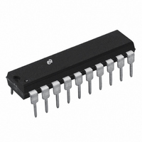
LMD18400N/NOPB National Semiconductor, LMD18400N/NOPB Datasheet - Page 14

LMD18400N/NOPB
Manufacturer Part Number
LMD18400N/NOPB
Description
IC DRIVER QUAD HI SIDE 20-DIP
Manufacturer
National Semiconductor
Datasheet
1.LMD18400NNOPB.pdf
(19 pages)
Specifications of LMD18400N/NOPB
Configuration
High-Side
Input Type
Non-Inverting
Delay Time
5µs
Current - Peak
3A
Number Of Configurations
4
Number Of Outputs
4
Voltage - Supply
7 V ~ 28 V
Operating Temperature
-25°C ~ 85°C
Mounting Type
Through Hole
Package / Case
20-DIP (0.300", 7.62mm)
Supply Voltage Min
7V
Supply Voltage Max
60V
No. Of Outputs
4
Output Voltage
5.5V
Output Current
3.75A
Driver Case Style
DIP
Msl
MSL 1 - Unlimited
Device Type
High Side
Rohs Compliant
Yes
Lead Free Status / RoHS Status
Lead free / RoHS Compliant
High Side Voltage - Max (bootstrap)
-
Other names
*LMD18400N
*LMD18400N/NOPB
LMD18400N
*LMD18400N/NOPB
LMD18400N
Available stocks
Company
Part Number
Manufacturer
Quantity
Price
Company:
Part Number:
LMD18400N/NOPB
Manufacturer:
National Semiconductor
Quantity:
135
www.national.com
Applications Information
When switched ON, the worst case power dissipation is:
The steady-state ON current of the inductor should be kept
less than 1A per power switch.
The additional power dissipation during turn-off, as the in-
ductor is de-energized and the voltage across the inductor is
clamped to −5V, can be found by:
FIGURE 12. Recommended PC Board Layout to Reduce the Thermal Resistance from Junction-to-Ambient
FIGURE 13. Switching an Inductive Load
(Continued)
01102623
01102621
14
for the time interval, t
inductor current to fall to zero:
The size of the inductor will determine the time duration for
this additional power dissipation interval. Even though the
peak current is kept less than 1A, the switch during this
interval will see a voltage across it of V
limit protection. If the inductor is too large, the time interval
may be long enough to heat the die temperature to +170˚C
thereby shutting OFF all other loads on the package.
The total average power dissipation during a full ON/OFF
switching cycle of an inductive load will be:
Due to the common cut-off of all loads forced by thermal
shutdown, the thermal time constants of the package be-
come a concern. Figure 14 provides an indication of the time
it takes to heat the die to thermal shutdown with a step
increase in package power dissipation from an initial junction
temperature of +25˚C. This data was measured using a PC
board layout providing a thermal resistance from junction to
ambient of approximately 35˚C/W. Less heatsinking will, of
course, result in faster thermal shutdown of the power
switches.
Maximum Power Dissipated
Thermal Resistance vs Size
and Junction to Ambient
CLAMP
. which is the time required for the
CC
+ 5V with no power
01102622


