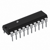
LMD18400N/NOPB National Semiconductor, LMD18400N/NOPB Datasheet - Page 9

LMD18400N/NOPB
Manufacturer Part Number
LMD18400N/NOPB
Description
IC DRIVER QUAD HI SIDE 20-DIP
Manufacturer
National Semiconductor
Datasheet
1.LMD18400NNOPB.pdf
(19 pages)
Specifications of LMD18400N/NOPB
Configuration
High-Side
Input Type
Non-Inverting
Delay Time
5µs
Current - Peak
3A
Number Of Configurations
4
Number Of Outputs
4
Voltage - Supply
7 V ~ 28 V
Operating Temperature
-25°C ~ 85°C
Mounting Type
Through Hole
Package / Case
20-DIP (0.300", 7.62mm)
Supply Voltage Min
7V
Supply Voltage Max
60V
No. Of Outputs
4
Output Voltage
5.5V
Output Current
3.75A
Driver Case Style
DIP
Msl
MSL 1 - Unlimited
Device Type
High Side
Rohs Compliant
Yes
Lead Free Status / RoHS Status
Lead free / RoHS Compliant
High Side Voltage - Max (bootstrap)
-
Other names
*LMD18400N
*LMD18400N/NOPB
LMD18400N
*LMD18400N/NOPB
LMD18400N
Available stocks
Company
Part Number
Manufacturer
Quantity
Price
Company:
Part Number:
LMD18400N/NOPB
Manufacturer:
National Semiconductor
Quantity:
135
Applications Information
1.3Ω (the ON resistance of the DMOS switch). The voltage
applied to the load will depend upon the load current and the
designed current capability of the LMD18400. When a switch
is commanded OFF, the load will be disconnected from the
supply except for a small leakage current of typically less
than 0.01 µA.
The LMD18400 can be continually connected to a live power
source, a car battery for example, while drawing less than
10 µA from the power source when put into a “sleep” condi-
tion. This “sleep” mode is enacted by taking the Enable Input
(pin 3) low. During this mode the supply current for the
device is typically only 0.04 µA. Special low current con-
sumption standby circuitry is used to hold the DMOS
switches OFF to eliminate the possibility of supply voltage
transients from turning on any of the loads (a common
problem with MOS power devices). When in the “sleep”
mode, all diagnostic and logic circuitry is inactive. When the
Enable Input is taken to a logic 1, the switches become
“armed” and ready to respond to their control input after a
short, 30 µs, enable delay time. This delay interval prevents
the switches from transient turn-on. Figure 2 shows the
switch control logic.
Each DMOS switch is turned ON when its gate is driven
approximately 3.5V more positive than its source voltage.
Because the source of the switch is the output terminal to the
load it can be taken to a voltage very near the V
potential. To ensure that there is sufficient voltage available
to drive the gates of the DMOS device a charge pump circuit
is built in. This circuit is controlled by an internal 300 kHz
oscillator and using an external 10 nF capacitor connected
from pin 14 to ground generates a voltage that is approxi-
mately 20V greater than the V
vides sufficient gate voltage drive for each of the switches
which is applied under command of standard 5V logic input
levels.
The turn-on time for each switch is approximately 12 µs
when driving a 1A load current. This relatively slow switching
time is beneficial in minimizing electromagnetic interference
(EMI) related problems created from switching high current
levels.
FIGURE 2. Control Logic for Each Power Switch
CC
supply voltage. This pro-
(Continued)
CC
supply
01102611
9
PROTECTION CIRCUITRY
The LMD18400 has extensive protection circuitry built in.
With any power device, protection against excessive volt-
age, current and temperature conditions is essential. To
achieve a “fail-safe” system implementation, the loads are
deactivated automatically by the LMD18400 in the event of
any detected overvoltage or over-temperature fault condi-
tions.
Voltage Protection
The V
any damage to the LMD18400. The CMOS logic circuitry is
biased from an internal 5.1V regulator which protects these
lower voltage transistors from the higher V
order to protect the loads connected to the switch outputs
however, an overvoltage shutdown circuit is employed.
Should the V
turned OFF thereby disconnecting the loads. This 35V
threshold has 750 mV of hysteresis to prevent potential
oscillations.
Additionally, there is an undervoltage lockout feature built in.
With V
logic circuitry can hold the switches in their commanded
state. To avoid this uncertainty, all of the switches are turned
OFF when V
illustrates the shutoff of an output during a 0V to 80V V
supply transient.
The LMD18400 has been designed to drive all types of
loads. When driving a ground referenced inductive load such
as a relay or solenoid, the voltage across the load will
reverse in polarity as the field in the inductor collapses when
the power switch is turned OFF. This will pull the output pin
of the LMD18400 below ground. This negative transient
voltage is clamped at approximately −5V to protect the IC.
This clamping action is not done with diodes but rather the
power DMOS switch turning back on momentarily to conduct
the inductor current as it de-energizes as shown in Figure 4.
FIGURE 3. Overvoltage/Undervoltage Shutdown
CC
CC
supply can range from −0.5V to +60 V
less than 5V it becomes uncertain whether the
CC
CC
potential exceed 35V all of the switches are
drops below approximately 5V. Figure 3
Voltage Shutdown
Over/Under
CC
01102612
potentials. In
www.national.com
DC
without
CC


