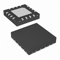
ISL6210CRZ Intersil, ISL6210CRZ Datasheet - Page 8

ISL6210CRZ
Manufacturer Part Number
ISL6210CRZ
Description
IC MOSFET DRIVER DUAL SYNC 16QFN
Manufacturer
Intersil
Datasheet
1.ISL6210CRZ.pdf
(10 pages)
Specifications of ISL6210CRZ
Configuration
High and Low Side, Synchronous
Input Type
PWM
Delay Time
26ns
Current - Peak
2A
Number Of Configurations
2
Number Of Outputs
4
High Side Voltage - Max (bootstrap)
36V
Voltage - Supply
4.5 V ~ 5.5 V
Operating Temperature
-10°C ~ 100°C
Mounting Type
Surface Mount
Package / Case
16-VQFN Exposed Pad, 16-HVQFN, 16-SQFN, 16-DHVQFN
Lead Free Status / RoHS Status
Lead free / RoHS Compliant
Available stocks
Company
Part Number
Manufacturer
Quantity
Price
Company:
Part Number:
ISL6210CRZ
Manufacturer:
NDK
Quantity:
3 924
Power Dissipation
Package power dissipation is mainly a function of the
switching frequency (F
external gate resistance, and the selected MOSFET’s
internal gate resistance and total gate charge. Calculating
the power dissipation in the driver for a desired application is
critical to ensure safe operation. Exceeding the maximum
allowable power dissipation level will push the IC beyond the
maximum recommended operating junction temperature of
+125°C. The maximum allowable IC power dissipation for
the SO14 package is approximately 1W at room
temperature, while the power dissipation capacity in the
QFN packages, with an exposed heat escape pad, is around
2W. See “Layout Considerations” on page 9 for thermal
transfer improvement suggestions. When designing the
driver into an application, it is recommended that the
following calculation is used to ensure safe operation at the
desired frequency for the selected MOSFETs. The total gate
drive power losses due to the gate charge of MOSFETs and
the driver’s internal circuitry and their corresponding average
driver current can be estimated with Equations 4 and 5,
respectively,
P
I
DR
Qg_TOT
FIGURE 4. BOOTSTRAP CAPACITANCE vs BOOT RIPPLE
P
P
=
Qg_Q2
Qg_Q1
2.0
1.8
1.6
1.4
1.2
1.0
0.8
0.6
0.4
0.2
0.0
⎛
⎜
⎝
Q
----------------------------- -
0.0
G1
20nC
=
V
GS1
P
•
=
=
0.1
Qg_Q1
VOLTAGE
N
Q
-------------------------------------- - F
Q
-------------------------------------- - F
Q1
G2
G1
0.2
Q
+
V
V
•
+
•
GATE
GS2
Q
----------------------------- -
GS1
PVCC
PVCC
P
G2
SW
V
0.3
Qg_Q2
GS2
= 100nC
•
), the output drive impedance, the
N
ΔV
2
2
0.4
Q2
•
BOOT_CAP
•
+
8
⎞
⎟
⎠
I
SW
Q
SW
•
0.5
F
•
SW
VCC
•
•
N
N
0.6
Q2
(V)
Q1
+
I
Q
0.7
0.8
0.9
(EQ. 5)
(EQ. 4)
1.0
ISL6210
where the gate charge (Q
particular gate to source voltage (V
corresponding MOSFET data sheet; I
quiescent current with no load at both drive outputs; N
and N
respectively. The I
the driver without capacitive load and is typically negligible.
The total gate drive power losses are dissipated among the
resistive components along the transition path. The drive
resistance dissipates a portion of the total gate drive power
losses, the rest will be dissipated by the external gate
resistors (R
interfering with the operation shoot-through protection
circuitry) and the internal gate resistors (R
MOSFETs. Figures 5 and 6 show the typical upper and lower
gate drives turn-on transition path. The power dissipation on
the driver can be roughly estimated as follows:
P
P
P
R
DR
DR_UP
DR_LOW
EXT2
FIGURE 6. TYPICAL LOWER-GATE DRIVE TURN-ON PATH
FIGURE 5. TYPICAL UPPER-GATE DRIVE TURN-ON PATH
PVCC
=
Q2
PVCC
P
=
DR_UP
=
are number of upper and lower MOSFETs,
R
=
⎛
⎜
⎝
G1
G1
--------------------------------------
R
⎛
⎜
⎝
R
HI1
--------------------------------------
R
R
+
and R
LO2
HI2
R
HI2
R
+
R
-------------
R
N
LO1
HI1
+
P
GI1
HI1
R
Q1
Q
DR_LOW
R
+
HI2
GND
V
EXT1
R
LGATE
G2
UGATE
PHASE
CC
EXT2
BOOT
, should be a short to avoid
product is the quiescent power of
G1
+
+
+
--------------------------------------- -
R
and Q
I
LO1
--------------------------------------- -
R
R
R
Q
LO2
G2
EXT2
R
•
R
G
G1
VCC
+
LO1
R
G
R
+
LO2
G2
GS1
R
C
EXT1
R
GI2
R
GD
=
C
Q
) is defined at a
EXT2
C
GI1
GD
R
GS
C
and V
is the driver’s total
G2
GS
⎞
⎟
⎠
GI1
•
⎞
⎟
⎠
S
+
P
---------------------
•
S
R
-------------
N
Qg_Q1
GS2
P
---------------------
and R
GI2
Qg_Q2
Q2
2
D
December 9, 2008
2
D
) in the
Q2
C
GI2
Q1
DS
C
FN6392.1
(EQ. 6)
DS
Q1
) of


