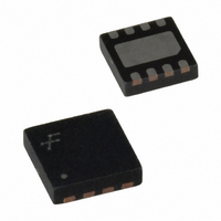
FAN5009MPX Fairchild Semiconductor, FAN5009MPX Datasheet - Page 8

FAN5009MPX
Manufacturer Part Number
FAN5009MPX
Description
IC DRIVER MOSFET DUAL 12V 8MLP
Manufacturer
Fairchild Semiconductor
Type
High Side/Low Sider
Specifications of FAN5009MPX
Configuration
High and Low Side, Synchronous
Input Type
Inverting and Non-Inverting
Delay Time
50ns
Number Of Configurations
1
Number Of Outputs
2
High Side Voltage - Max (bootstrap)
15V
Voltage - Supply
6.4 V ~ 13.5 V
Operating Temperature
0°C ~ 85°C
Mounting Type
Surface Mount
Package / Case
8-MLP
Supply Voltage (min)
10 V
Supply Current
8 mA
Maximum Power Dissipation
715 mW
Maximum Operating Temperature
+ 85 C
Mounting Style
SMD/SMT
Minimum Operating Temperature
0 C
Number Of Drivers
2
Lead Free Status / RoHS Status
Lead free / RoHS Compliant
Current - Peak
-
Lead Free Status / Rohs Status
Lead free / RoHS Compliant
FAN5009
Circuit Description
The FAN5009 is a dual MOSFET driver optimized for driv-
ing N-channel MOSFETs in a synchronous buck converter
topology. A single PWM input signal is all that is required to
properly drive the high-side and the low-side MOSFETs.
Each driver is capable of driving a 3nF load at speeds up to
500kHz.
For a more detailed description of the FAN5009 and its
features, refer to the Internal Block Diagram and Figure 1.
Low-Side Driver
The low-side driver (LDRV) is designed to drive a ground-
referenced low R
LDRV is internally connected between VCC and PGND.
When the driver is enabled, the driver’s output is 180° out of
phase with the PWM input. When the FAN5009 is disabled
(OD = 0V), LDRV is held low.
High-Side Driver
The high-side driver (HDRV) is designed to drive a floating
N-channel MOSFET. The bias voltage for the high-side
driver is developed by a bootstrap supply circuit, consisting
of the internal diode and external bootstrap capacitor
(C
During start-up, SW is held at PGND, allowing C
charge to VCC through the internal diode. When the PWM
input goes high, HDRV will begin to charge the high-side
MOSFET’s gate (Q1). During this transition, charge is
removed from C
turns on, SW rises to V
V
for Q1.
To complete the switching cycle, Q1 is turned off by pulling
HDRV to SW. C
falls to PGND.
HDRV output is in phase with the PWM input. When the
driver is disabled, the high-side gate is held low.
Adaptive Gate Drive Circuit
The FAN5009 embodies an advanced design that ensures
minimum MOSFET dead-time while eliminating potential
shoot-through (cross-conduction) currents. It senses the
state of the MOSFETs and adjusts the gate drive, adaptively,
to ensure they do not conduct simultaneously. Refer to
Figure 4 for the relevant timing waveforms.
To prevent overlap during the low-to-high switching transi-
tion (Q2 OFF to Q1 ON), the adaptive circuitry monitors the
voltage at the LDRV pin. When the PWM signal goes
HIGH, Q2 will begin to turn OFF after some propagation
delay (t
8
IN
BOOT
+V
C(BOOT)
pdl(LDRV)
) .
, which provides sufficient V
BOOT
BOOT
).
DS(on)
and delivered to Q1’s gate. As Q1
is then recharged to VCC when SW
IN
N-channel MOSFETs. The bias for
, forcing the BOOT pin to
GS
enhancement
BOOT
to
Once the LDRV pin is discharged below ~1.2V, Q1 begins to
turn ON after adaptive delay t
To preclude overlap during the high-to-low transition (Q1
OFF to Q2 ON), the adaptive circuitry monitors the voltage
at the SW pin. When the PWM signal goes LOW, Q1 will
begin to turn OFF after some propagation delay (t
Once the SW pin falls below ~2.2V, Q2 begins to turn ON
after adaptive delay t
Additionally, V
discharged below ~1.2V, a secondary adaptive delay is initi-
ated, which results in Q2 being driven ON after t
regardless of SW state. This function is implemented to
ensure C
for cases where the power convertor is sinking current and
SW voltage does not fall below the 2.2V adaptive threshold.
Secondary delay t
Application Information
Supply Capacitor Selection
For the supply input (V
bypass capacitor is recommended to reduce the noise and to
supply the peak current. Use at least a 1µF, X7R or X5R
capacitor. Keep this capacitor close to the FAN5009 V
and PGND pins.
Bootstrap Circuit
The bootstrap circuit uses a charge storage capacitor
(C
tion of these components should be done after the high-side
MOSFET has been chosen. The required capacitance is
determined using the following equation:
where Q
and ∆V
MOSFET drive. For example, the Q
about 35nC @ 12V
required bootstrap capacitance is 100nF. A good quality
ceramic capacitor must be used.
The average diode forward current, I
estimated by:
where F
The peak surge current rating of the internal diode should be
checked in-circuit, since this is dependent on the equivalent
impedance of the entire bootstrap circuit, including the PCB
traces. For applications requiring higher I
diode may be used in parallel to the internal diode.
BOOT
I
F AVG
C
(
BOOT
BOOT
) and the internal diode, as shown in Figure 1. Selec-
SW
G
BOOT
is the total gate charge of the high-side MOSFET,
)
is the switching frequency of the controller.
=
=
is the voltage droop allowed on the high-side
is recharged each switching cycle, particularly
Q
GS
--------------------- -
∆V
GATE
pdh(ODRV)
Q
of Q1 is monitored. When V
BOOT
GS
G
pdh(LDRV)
. For an allowed droop of ~300mV, the
×
CC
F
SW
) of the FAN5009, a local ceramic
is longer than t
pdh(HDRV)
.
PRODUCT SPECIFICATION
G
F(AVG)
of the FDD6696 is
.
REV. 1.0.5 7/22/04
F
, an external
, can be
pdh(LDRV)
GS(Q1)
pdh(ODRV)
pdl(HDRV)
.
is
CC
(2)
(1)
).
,


