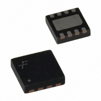
FAN5009MPX Fairchild Semiconductor, FAN5009MPX Datasheet - Page 9

FAN5009MPX
Manufacturer Part Number
FAN5009MPX
Description
IC DRIVER MOSFET DUAL 12V 8MLP
Manufacturer
Fairchild Semiconductor
Type
High Side/Low Sider
Specifications of FAN5009MPX
Configuration
High and Low Side, Synchronous
Input Type
Inverting and Non-Inverting
Delay Time
50ns
Number Of Configurations
1
Number Of Outputs
2
High Side Voltage - Max (bootstrap)
15V
Voltage - Supply
6.4 V ~ 13.5 V
Operating Temperature
0°C ~ 85°C
Mounting Type
Surface Mount
Package / Case
8-MLP
Supply Voltage (min)
10 V
Supply Current
8 mA
Maximum Power Dissipation
715 mW
Maximum Operating Temperature
+ 85 C
Mounting Style
SMD/SMT
Minimum Operating Temperature
0 C
Number Of Drivers
2
Lead Free Status / RoHS Status
Lead free / RoHS Compliant
Current - Peak
-
Lead Free Status / Rohs Status
Lead free / RoHS Compliant
PRODUCT SPECIFICATION
Thermal Considerations
Total device dissipation:
where P
where F
P
Where Q
it’s applied V
V
using the datasheet curves, where:
P
FET driver.
Where P
rising and falling edges, respectively:
where:
As described in eq. 8 and 9 above, the total power consumed
in driving the gate is divided in proportion to the resistances
in series with the MOSFET's internal gate node as shown
below:
REV. 1.0.5 7/22/04
R
HDRV
F
is power dissipated in the bootstrap rectifier:
for the applied I
P
I
Q1
P
P
P
P
P
P
F AVG
represents internal power dissipation of the upper
D
Q
R
HDRV
H R
H F ( )
(
Q
SW
H(R)
G1
( )
BOOT
=
=
represents quiescent power dissipation:
=
=
is switching frequency (in kHz).
is total gate charge of the upper FET (Q1) for
1
-- -
2
P
V
V
)
Figure 5. Driver dissipation model
=
=
GS
R
R
and P
Q
CC
F
=
×
=
HUP
HDN
×
P
.
P
HDRV
+
Q
P
F
Q1
×
Q1
F
P
G1
SW
SW
H R
SW
[
R
F(AVG)
H(F)
( )
4mA + 0.036 F
×
×
×
+
×
---------------------------------------- -
R
×
----------------------------------------
R
+
V
P
Q
HDN
Q
HUP
GS Q1
HDRV
P
are internal dissipations for the
G1
G1
H F ( )
can be graphically determined
(
R
R
R
+
+
E
HDN
HUP
+
)
R
R
×
P
E
E
F
(
LDRV
G
+
+
SW
SW
R
R
G
G
R
–
G
100
Q1
)
]
S
(10)
(4)
(5)
(7)
(3)
(6)
(8)
(9)
R
R
designs. Note that the introduction of R
power dissipation, but excess R
“adaptive gate drive” circuitry. For more information please
refer to Fairchild app note AN-6003, “Shoot-through” in
Synchronous Buck Converters.
P
Where P
rising and falling edges, respectively:
where:
Layout Considerations
Use the following general guidelines when designing printed
circuit boards (see Figures 6 and 7):
1.
2.
3.
4.
LDRV
G
E
is the external gate drive resistor implemented in many
is the polysilicon gate resistance, internal to the FET.
P
Trace out the high-current paths and use short, wide
(>25 mil) traces to make these connections.
Connect the PGND pin of the FAN5009 as close as
possible to the source of the lower MOSFET.
The V
possible to V
Use vias to other layers when possible to maximize
thermal conduction away from the IC.
recommendation for SO8 package (not to scale)
P
Q2
P
P
LDRV
is dissipation of the lower FET driver.
L F ( )
L R
H(R)
Figure 6. External component placement
( )
=
CC
1
-- -
2
=
=
=
and P
1
2
3
4
bypass capacitor should be located as close as
×
C
P
P
P
Q
VCC
L R
Q2
Q2
CC
G2
( )
H(F)
×
×
×
and PGND pins.
+
---------------------------------------- -
R
C
--------------------------------------- -
R
V
P
HDN
BOOT
LUP
GS Q2
L F ( )
are internal dissipations for the
(
R
R
+
+
LDN
LUP
R
)
R
E
×
E
E
may cause errors in the
F
+
+
SW
R
R
8
7
6
5
G
G
E
can reduce driver
FAN5009
(11)
(12)
(13)
(14)
9


