IXBD4411PI IXYS, IXBD4411PI Datasheet
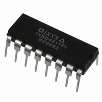
IC HIGH SIDE DRIVER 16DIP

IXBD4411PI

Manufacturer Part Number
IXBD4411PI
Description
IC HIGH SIDE DRIVER 16DIP
Manufacturer
IXYS
Series
ISOSMART™r
Type
Isolated Half Bridge Driver Chip Setr
Datasheet

Specifications of IXBD4411PI

Configuration
High-Side
Input Type
Non-Inverting
Delay Time
110ns
Current - Peak
2A
Number Of Configurations
1
Number Of Outputs
1
High Side Voltage - Max (bootstrap)
1200V
Voltage - Supply
10 V ~ 20 V
Operating Temperature
-40°C ~ 85°C
Mounting Type
Through Hole
Package / Case
16-DIP (0.300", 7.62mm)
Product
Half-Bridge Drivers
Rise Time
100 ns
Fall Time
150 ns
Supply Voltage (min)
10 V
Maximum Power Dissipation
600 mW
Maximum Operating Temperature
+ 85 C
Mounting Style
Through Hole
Bridge Type
Half Bridge
Minimum Operating Temperature
- 40 C
Number Of Drivers
1
Output Current
2 A
Lead Free Status / RoHS Status
Lead free / RoHS Compliant
The IXBD4410/IXBD4411 ISOSMART
chipset is designed to control the gates
of two Power MOSFETs or Power
IGBTs that are connected in a half-
bridge (phase-leg) configuration for
driving multiple-phase motors, or used
in applications that require half-bridge
power circuits. The IXBD4410/
IXBD4411 is a full-feature chipset
consisting of two 16-Pin DIP or SO
devices interfaced and isolated by two
small-signal ferrite pulse transformers.
The small-signal transformers provide
greater than 1200 V isolation.
Even with commutating noise ambients
greater than ±50 V/ns and up to 1200 V
potentials, this chipset establishes
error-free two-way communications
between the system ground-reference
IXBD4410 and the inverter output-
IXYS reserves the right to change limits, test conditions and dimensions.
© 2004 IXYS All rights reserved
ISOSMART
Type
IXBD4410PI
IXBD4411PI
IXBD4410SI
IXBD4411SI
Description
Full-Feature Low-Side Driver 16-Pin P-DIP
Full-Feature High-Side Driver 16-Pin P-DIP
Full-Feature Low-Side Driver 16-Pin SO
Full-Feature High-Side Driver 16-Pin SO
TM
Half Bridge Driver Chipset
reference IXBD4411. They incorporate
undervoltage V
overcurrent or desaturation shutdown
to protect the IGBT or Power MOSFET
devices from damage.
The chipset provides the necessary
gate drive signals to fully control the
grounded-source low-side power
device as well as the floating-source
high-side power device. Additionally,
the IXBD4410/4411 chipset provides a
negative-going, off-state gate drive
signal for improved turn-off of IGBTs or
Power MOSFETs and a system logic-
compatible status fault output FLT to
indicate overcurrent or desaturation,
and undervoltage V
status fault, both chipset keep their
respective gate drive outputs off; at
V
EE
540 V-
.
Package
DD
or V
DD
Temperature Range
EE
or V
-40 to +85°C
-40 to +85°C
-40 to +85°C
-40 to +85°C
lockout and
EE
. During a
Features
Applications
1- or 3-Phase Motor Controls
Switch Mode Power Supplies
(SMPS)
Uninterruptible Power Supplies
(UPS)
Induction Heating and Welding
Systems
Switching Amplifiers
General Power Conversion Circuits
1200 V or greater low-to-high side
isolation.
Drives Power Systems Operating on
up to 575 V AC mains
dv/dt immunity of greater than
±50V/ns
Proprietary low-to-high side level
translation and communication
On-chip negative gate-drive supply
to ensure Power MOSFET or IGBT
turn-off and to prevent gate noise
interference
5 V logic compatible HCMOS inputs
with hysteresis
Available in either the 16-Pin DIP or
the 16-Pin wide-body, small-outline
plastic package
20 ns switching time with 1000 pF
load; 100 ns switching time with
10,000 pF load
100 ns propagation delay time
2 A peak output drive capability
Self shut-down of output in response
to over-current or short-circuit
Under-voltage and over-voltage V
lockout protection
Protection from cross conduction of
the half bridge
Logic compatible fault indication
from both low and high-side driver
IXBD4410
IXBD4411
1
DD

Related parts for IXBD4411PI

IXBD4411PI Summary of contents

Page 1

... ISOSMART Half Bridge Driver Chipset TM Type Description IXBD4410PI Full-Feature Low-Side Driver 16-Pin P-DIP IXBD4411PI Full-Feature High-Side Driver 16-Pin P-DIP IXBD4410SI Full-Feature Low-Side Driver 16-Pin SO IXBD4411SI Full-Feature High-Side Driver 16-Pin SO The IXBD4410/IXBD4411 ISOSMART chipset is designed to control the gates of two Power MOSFETs or Power ...

Page 2

... EE 600 -3 -4.8 Dimensions in inch (1" = 25.4 mm) 16-Pin SOIC V +0 °C °C °C °C K/W Die substrate K/W connected to tab 16-Pin Plastic DIP 1 µ Ω 4 Ω A End view V pF Ω kHz V © 2004 IXYS All rights reserved IXBD4410 IXBD4411 ...

Page 3

... Fault Output Delay for any Fault Conditions (4410/4411) t FLT Delay kΩ C FLT pu Overcurrent Protection Delay t Driver-Off delay time C oc Fig. 1a: IXBD4410/4411 Switching time test circuit © 2004 IXYS All rights reserved Characteristic Values = 25° unless otherwise specified) DD min. typ. 9.5 10.5 0.1 0.15 ...

Page 4

... The fault signal that is returned from Fig. 2: IXBD4411, high-side driver block diagram Fig. 3: IXBD4410, low-side driver block diagram Fig. 4: Logic representation of IXBD4410 FLT signal IXBD4410 IXBD4411 © 2004 IXYS All rights reserved ...

Page 5

... Miller capaci- tance or from inductive ground transients. These charge pumps provide -5 V relative to the local driver ground when © 2004 IXYS All rights reserved +15 V, and at rated average DD currents of 25 mA. The charge pump requires two external capacitors, C7 and C11 in Fig ...

Page 6

... IXBD4411, this output responds to the transmitted signal from the companion IXBD4410. A "high" at INH of the IXBD4410 drives will turn it on ("high"). A "low" will turn it off ("low"). This output will turn off ("low") also in response to any fault condition. © 2004 IXYS All rights reserved IXBD4410 IXBD4411 ...

Page 7

... Q1. This dv/dt is impressed across the Miller capacitance of Q1, forcing a large current to flow out the gate © 2004 IXYS All rights reserved Fig. 5: Switching a clamped inductive load terminal of the device. If this current pulse causes a high enough voltage ...

Page 8

... DC bus potential. To keep this normal condition from setting the internal fault flip-flop of the IXBD4410 or the IXBD4411, an internal CMOS switch is turned on and placed across lM and KG pins shorting them together. This effectively discharges C8 or C12 in Fig. 6 and maintains zero potential © 2004 IXYS All rights reserved R s ...

Page 9

... IXBD4410/4411 and its associated circuitry. © 2004 IXYS All rights reserved Fig. 8: Typical 3-phase motor control system block diagram PCB Layout Considerations The IXBD4410/4411 is intended to be used in high voltage, high speed, high dv/dt applications ...

Page 10

... AWG magnet wire are made. The two windings are segment wound to achieve primary-to- secondary isolation 2500 V~. The six-turn primaries are connected to the respective IXBD4410/4411 transmitter outputs and the two-turn secondaries are connected to their respective receiver inputs. © 2004 IXYS All rights reserved ...

Page 11

... The resistor will control the damping of the signal and limit the peak transmitter output current. The receiver is designed to operate © 2004 IXYS All rights reserved 6:2 Fig. 11: Ferrite bead dimensions 125 over a wide common mode input range. ...

Related keywords