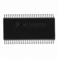
MCZ33927EK Freescale Semiconductor, MCZ33927EK Datasheet - Page 20

MCZ33927EK
Manufacturer Part Number
MCZ33927EK
Description
IC FET PRE-DRIVER 3PH 54-SOIC
Manufacturer
Freescale Semiconductor
Specifications of MCZ33927EK
Configuration
3 Phase Bridge
Input Type
Inverting and Non-Inverting
Delay Time
265ns
Current - Peak
600mA
Number Of Configurations
1
Number Of Outputs
3
High Side Voltage - Max (bootstrap)
75V
Voltage - Supply
8 V ~ 40 V
Operating Temperature
-40°C ~ 125°C
Mounting Type
Surface Mount
Package / Case
54-SOIC (7.5mm Width) Exposed Pad, 54-eSOIC, 54-HSOIC
Lead Free Status / RoHS Status
Lead free / RoHS Compliant
Available stocks
Company
Part Number
Manufacturer
Quantity
Price
large FETs used to drive three-phase loads. A typical load
FET may have an on-resistance of 4.0m Ω or less and could
require a gate charge of over 400 nC to fully turn on. The IC
can operate in automotive 12V to 42V environments.
PHASE A (PHASEA)
comparator. This output is low when the voltage on Phase A
high-side source (source of the High-Side load FET) is less
than 50 percent of VBAT.
POWER GROUND (PGND)
connected to VSS, however routing to a single point ground
on the PCB may help to isolate charge pump noise.
each of the Phases.
ENABLE 1 AND ENABLE 2 (EN1, EN2)
any gate drive output. When either or both are low, the
internal logic (SPI port, etc.) still functions normally, but all
gate drives are forced off (external power FET gates pulled
low). The signal is asynchronous.
each LS driver must be pulsed on before the corresponding
HS driver can be commanded on. This ensures that the
bootstrap capacitors are charged.
RESET (RST)
low power state. In this mode all outputs are disabled, internal
bias circuits are turned off, and a small pull down current is
applied to the output gate drives. The internal logic will be
reset within 77ns of RESET going low. When RST is low, the
IC will consume minimal current.
CHARGE PUMP OUT (PUMP)
The output of the internal charge pump support circuit. When
the charge pump is used, it is connected to the external
pumping capacitor. This pin may be left floating if the charge
pump is not required.
20
33927
FUNCTIONAL DESCRIPTIONS
INTRODUCTION
The 33927 provides an interface between an MCU and the
This pin is the totem pole output of the Phase A
This pin is power ground for the charge pump. It should be
NOTE: This is NOT the same as the Phase Grounds for
Both of these logic signal inputs must be high to enable
When EN1 and EN2 return high to enable the outputs,
When the reset pin is low the integrated circuit (IC) is in a
This input should not be driven above the VDD voltage.
This pin is the switching node of the charge pump circuit.
FUNCTIONAL DESCRIPTIONS
FUNCTIONAL PIN DESCRIPTION
INTRODUCTION
phase systems, the IC enforces few constraints on driving the
FETs. It does provide deadtime (cross-over) blanking and
logic, both of which can be overridden, ensuring both FETs in
a phase are not simultaneously enabled.
CHARGE PUMP INPUT (VPUMP)
When the charge pump is required, this pin should be
connected to a polarity protected supply. Typical applications
would connect it to VBAT. This input should never be
connected to a supply greater than 40V.
floating.
VBAT INPUT (VBAT)
voltage. It is used to provide power to the internal steady
state trickle charge pump and to energize the hold-off circuit.
It is also the reference bias for the Phase Comparators and
Desaturation Comparator.
PHASE B (PHASEB)
comparator. This output is low when the voltage on Phase B
high-side source (source of the High-Side load FET) is less
than 50 percent of VBAT.
PHASE C (PHASEC)
comparator. This output is low when the voltage on Phase C
high-side source (source of the High-Side load FET) is less
than 50 percent of VBAT.
PHASE A HIGH-SIDE INPUT (PA_HS)
Phase A. The signal is active low, and is pulled up by an
internal current source.
PHASE A LOW-SIDE INPUT (PA_LS)
Phase A. The signal is active high, and is pulled down by an
internal current sink.
VDD VOLTAGE REGULATOR (VDD)
regulator provides continuous power to the IC and is a supply
Because there are so many methods of controlling three-
A SPI port is used to configure the IC modes.
This pin is the input supply for the charge pump circuit.
If the charge pump is not required this pin may be left
This pin should be connected to the system battery
This pin is the totem pole output of the Phase B
This pin is the totem pole output of the Phase C
This input logic signal pin enables the High-Side Driver for
This input logic signal pin enables the Low-Side Driver for
This pin is an internally generated 5V supply. The internal
Analog Integrated Circuit Device Data
Freescale Semiconductor


