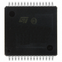
VND5004ASP30TR-E STMicroelectronics, VND5004ASP30TR-E Datasheet - Page 18

VND5004ASP30TR-E
Manufacturer Part Number
VND5004ASP30TR-E
Description
IC DRIVER HIGH SIDE 30-MPSO
Manufacturer
STMicroelectronics
Type
High Sider
Datasheet
1.VND5004ASP30TR-E.pdf
(34 pages)
Specifications of VND5004ASP30TR-E
Input Type
Non-Inverting
Number Of Outputs
2
On-state Resistance
4 mOhm
Current - Peak Output
100A
Voltage - Supply
4.5 V ~ 27 V
Operating Temperature
-40°C ~ 150°C
Mounting Type
Surface Mount
Package / Case
30-MPSO, MultiPowerSO
Product
Driver ICs - Various
Supply Voltage (min)
4.5 V
Supply Current
6 mA
Maximum Operating Temperature
+ 150 C
Mounting Style
SMD/SMT
Maximum Turn-off Delay Time
35000 ns
Maximum Turn-on Delay Time
25000 ns
Minimum Operating Temperature
- 40 C
Number Of Drivers
2
Driver Configuration
Non-Inverting
Driver Type
High Side
Input Logic Level
CMOS
Operating Supply Voltage (max)
27V
Operating Supply Voltage (min)
4.5V
Operating Supply Voltage (typ)
13V
Turn Off Delay Time
35us
Turn On Delay Time (max)
25us
Operating Temp Range
-40C to 150C
Operating Temperature Classification
Automotive
Mounting
Surface Mount
Pin Count
30
Package Type
MultiPowerSO
Lead Free Status / RoHS Status
Lead free / RoHS Compliant
Current - Output / Channel
-
Lead Free Status / Rohs Status
Lead free / RoHS Compliant
Available stocks
Company
Part Number
Manufacturer
Quantity
Price
Part Number:
VND5004ASP30TR-E
Manufacturer:
ST
Quantity:
20 000
Application information
3
3.1
3.2
18/34
Application information
Figure 22. Application schematic
MCU I/Os protection
When negative transients are present on the V
negative to approximately -1.5V.
ST suggests the insertion of resistors (R
latching up.
The values of these resistors provide a compromise between the leakage current of the µC,
the current required by the HSD I/Os (input levels compatibility) and the latch-up limit of the
µC I/Os.
-V
Calculation example:
For V
75Ω ≤ R
Recommended values: R
Load dump protection
D
V
line that are greater than the ones shown in the ISO 7637-2: 2004(E) table.
CCPK
ld
CCpeak
is necessary (Voltage Transient Suppressor) if the load dump peak voltage exceeds the
+5V
µC
CCpeak
max rating. The same applies if the device will be subject to transients on the V
prot
/I
latchup
≤ 240kΩ .
= - 1.5V and I
C
ext
≤ R
R
R
R
prot
prot
R
prot
prot
SENSE
≤ (V
prot
latchup
OHµC
CURRENT SENSE
=10kΩ, C
CS_DIS
INPUT
-V
≥ 20mA; V
45V
IH
) / I
IHmax
EXT =
prot
OHµC
) in the lines to prevent the µC I/Os pins from
10nF
CC
≥ 4.5V
line, the control pins will be pulled
GND
VND5004A-E / VND5004ASP30-E
20V
V
CC
OUTPUT
D
ld
CC


