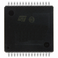
VND5004ASP30TR-E STMicroelectronics, VND5004ASP30TR-E Datasheet - Page 5

VND5004ASP30TR-E
Manufacturer Part Number
VND5004ASP30TR-E
Description
IC DRIVER HIGH SIDE 30-MPSO
Manufacturer
STMicroelectronics
Type
High Sider
Datasheet
1.VND5004ASP30TR-E.pdf
(34 pages)
Specifications of VND5004ASP30TR-E
Input Type
Non-Inverting
Number Of Outputs
2
On-state Resistance
4 mOhm
Current - Peak Output
100A
Voltage - Supply
4.5 V ~ 27 V
Operating Temperature
-40°C ~ 150°C
Mounting Type
Surface Mount
Package / Case
30-MPSO, MultiPowerSO
Product
Driver ICs - Various
Supply Voltage (min)
4.5 V
Supply Current
6 mA
Maximum Operating Temperature
+ 150 C
Mounting Style
SMD/SMT
Maximum Turn-off Delay Time
35000 ns
Maximum Turn-on Delay Time
25000 ns
Minimum Operating Temperature
- 40 C
Number Of Drivers
2
Driver Configuration
Non-Inverting
Driver Type
High Side
Input Logic Level
CMOS
Operating Supply Voltage (max)
27V
Operating Supply Voltage (min)
4.5V
Operating Supply Voltage (typ)
13V
Turn Off Delay Time
35us
Turn On Delay Time (max)
25us
Operating Temp Range
-40C to 150C
Operating Temperature Classification
Automotive
Mounting
Surface Mount
Pin Count
30
Package Type
MultiPowerSO
Lead Free Status / RoHS Status
Lead free / RoHS Compliant
Current - Output / Channel
-
Lead Free Status / Rohs Status
Lead free / RoHS Compliant
Available stocks
Company
Part Number
Manufacturer
Quantity
Price
Part Number:
VND5004ASP30TR-E
Manufacturer:
ST
Quantity:
20 000
VND5004A-E / VND5004ASP30-E
1
Block diagram and pin configurations
Figure 1.
Table 2.
CURRENT SENSE1,2 Analog current sense pin, delivers a current proportional to the load current
INPUT1
INPUT2
CS_DIS
OUTPUT1,2
GND
INPUT1,2
CS_DIS
Name
GND
VCC
Block diagram
Pin functions
Reverse
battery
protection
V
clamp
CC
Battery connection
Power output
Ground connection
Voltage controlled input pin with hysteresis, CMOS compatible. Controls
output switch state
Active high CMOS compatible pin, to disable the current sense pins
LOGIC
voltage
Under
Pwr
Pwr
LIM
LIM
DRIVER
DRIVER
Overtemp.
Overtemp.
Block diagram and pin configurations
Function
CS_DIS
CS_DIS
I
I
OUT1
OUT2
PwCLAMP
PwCLAMP
I
I
LIM
LIM
K
K
V
CC
CURRENT
SENSE1
CURRENT
SENSE2
OUTPUT1
OUTPUT2
5/34


