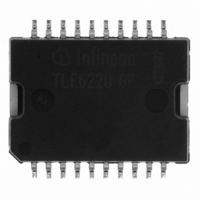
TLE6220GP Infineon Technologies, TLE6220GP Datasheet - Page 5

TLE6220GP
Manufacturer Part Number
TLE6220GP
Description
IC SW SMART QUAD LOSIDE DSO-20
Manufacturer
Infineon Technologies
Type
Low Sider
Datasheet
1.TLE6220GP.pdf
(19 pages)
Specifications of TLE6220GP
Input Type
SPI
Number Of Outputs
4
On-state Resistance
320 mOhm
Current - Output / Channel
3A
Current - Peak Output
6A
Voltage - Supply
4.5 V ~ 5.5 V
Operating Temperature
-40°C ~ 150°C
Mounting Type
Surface Mount
Package / Case
DSO-20
Switch Type
Low Side
Power Switch Family
TLE6220GP
Input Voltage
-0.3 to 7V
Power Switch On Resistance
320mOhm
Output Current
3A
Mounting
Surface Mount
Supply Current
1mA
Package Type
DSO
Operating Temperature (min)
-40C
Operating Temperature (max)
150C
Operating Temperature Classification
Automotive
Pin Count
22
Power Dissipation
3W
Packages
PG-DSO-20
Thermal Class
Heatslug down
Id Nom
4 x 1 A
Channels
4.0
Comment
inductive and resistive loads (e.g. injectors)
Lead Free Status / RoHS Status
Lead free / RoHS Compliant
Other names
SP000011903
SP000308873
TLE6220GPINTR
TLE6220GPNT
TLE6220GPT
TLE6220GPT
TLE6220GPXT
SP000308873
TLE6220GPINTR
TLE6220GPNT
TLE6220GPT
TLE6220GPT
TLE6220GPXT
Available stocks
Company
Part Number
Manufacturer
Quantity
Price
Company:
Part Number:
TLE6220GP
Manufacturer:
INFINEON
Quantity:
7 154
Company:
Part Number:
TLE6220GP
Manufacturer:
INFINEON
Quantity:
703
Part Number:
TLE6220GP
Manufacturer:
INFINEON/英飞凌
Quantity:
20 000
Part Number:
TLE6220GPAUMA2
Manufacturer:
INFINEON/英飞凌
Quantity:
20 000
Electrical Characteristics cont.
Parameter and Conditions
V
(unless otherwise specified)
5. Diagnostic Functions
Open Load Detection Voltage
Output Pull Down Current
Fault Delay Time
Short to Ground Detection Voltage
Short to Ground Detection Current
6. SPI-Timing
Serial Clock Frequency (depending on SO load)
Serial Clock Period (1/fclk)
Serial Clock High Time
Serial Clock Low Time
Enable Lead Time (falling edge of
CLK
Enable Lag Time (falling edge of CLK to rising edge of
Data Setup Time (required time SI to falling of CLK)
Data Hold Time (falling edge of CLK to SI)
Disable Time @ C
Transfer Delay Time
(
Data Valid Time
7
8
V2.2
CS
This time is necessary between two write accesses. To get the correct diagnostic information, the transfer delay
This parameter will not be tested but guaranteed by design
time has to be extended to the maximum fault delay time t
S
= 4.5 to 5.5 V ; T
)
high time between two accesses)
L
= 50 pF
j
7
= - 40 °C to + 150 °C ; Reset = H
8
CS
to rising edge of
C
C
C
L
L
L
Page
= 50 pF
= 100 pF
= 220 pF
d(fault)max
CS
5
8
8
) t
Symbol
V
I
t
V
I
f
t
t
t
t
t
t
t
t
t
PD(OL)
d(fault)
SHG
SCK
p(SCK)
SCKH
SCKL
lead
lag
SU
H
DIS
dt
valid
= 200µs.
DS(OL)
DS(SHG)
Data Sheet TLE 6220 GP
Values
V
V
50
50
-50
DC
200
50
50
250
250
20
20
--
200
--
--
--
S
S
min
-2.5 V
–3.3 V
90
110
-100
--
--
--
--
--
---
--
--
--
--
--
--
--
S
S
typ
-2.9 V
-2
V
150
200
-150
5
--
--
--
--
--
--
--
150
--
110
120
150
S
S
max
-1.3
-2.5
2009-11-18
Unit
MHz
ns
ns
ns
ns
ns
ns
ns
ns
ns
ns
µA
µA
µs
V
V


