TLE6220GP Infineon Technologies, TLE6220GP Datasheet - Page 6
TLE6220GP
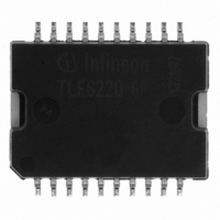
Manufacturer Part Number
TLE6220GP
Description
IC SW SMART QUAD LOSIDE DSO-20
Manufacturer
Infineon Technologies
Type
Low Sider
Datasheet
1.TLE6220GP.pdf
(19 pages)
Specifications of TLE6220GP
Input Type
SPI
Number Of Outputs
4
On-state Resistance
320 mOhm
Current - Output / Channel
3A
Current - Peak Output
6A
Voltage - Supply
4.5 V ~ 5.5 V
Operating Temperature
-40°C ~ 150°C
Mounting Type
Surface Mount
Package / Case
DSO-20
Switch Type
Low Side
Power Switch Family
TLE6220GP
Input Voltage
-0.3 to 7V
Power Switch On Resistance
320mOhm
Output Current
3A
Mounting
Surface Mount
Supply Current
1mA
Package Type
DSO
Operating Temperature (min)
-40C
Operating Temperature (max)
150C
Operating Temperature Classification
Automotive
Pin Count
22
Power Dissipation
3W
Packages
PG-DSO-20
Thermal Class
Heatslug down
Id Nom
4 x 1 A
Channels
4.0
Comment
inductive and resistive loads (e.g. injectors)
Lead Free Status / RoHS Status
Lead free / RoHS Compliant
Other names
SP000011903
SP000308873
TLE6220GPINTR
TLE6220GPNT
TLE6220GPT
TLE6220GPT
TLE6220GPXT
SP000308873
TLE6220GPINTR
TLE6220GPNT
TLE6220GPT
TLE6220GPT
TLE6220GPXT
Available stocks
Company
Part Number
Manufacturer
Quantity
Price
Company:

Part Number:
TLE6220GP
Manufacturer:
INFINEON
Quantity:
7 154
Company:
Part Number:
TLE6220GP
Manufacturer:
INFINEON
Quantity:
703
Part Number:
TLE6220GP
Manufacturer:
INFINEON/英飞凌
Quantity:
20 000
Part Number:
TLE6220GPAUMA2
Manufacturer:
INFINEON/英飞凌
Quantity:
20 000


Functional Description
The TLE 6220 GP is an quad-low-side power switch which provides a serial peripheral inter-
face (SPI) to control the 4 power DMOS switches, as well as diagnostic feedback. The power
transistors are protected against short to V
voltage by an active zener clamp.
The diagnostic logic recognises a fault condition which can be read out via the serial diagnos-
tic output (SO).
Circuit Description
Power Transistor Protection Functions
Each of the four output stages has its own zener clamp, which causes a voltage limitation at
the power transistor when solenoid loads are switched off. The outputs are provided with a
current limitation set to a minimum of 3 A. The continuous current for each channel is 1A (all
channels ON; depending on cooling).
Each output is protected by embedded protection functions. In the event of an overload or
short to supply, the current is internally limited and the corresponding bit combination is set
(early warning). If this operation leads to an overtemperature condition, a second protection
level (about 170 °C) will change the output into a low duty cycle PWM (selective thermal shut-
down with restart) to prevent critical chip temperatures.
SPI Signal Description
pin. Whenever the pin is in a logic low state, data can be transferred from the µC and vice
versa.
To avoid any false clocking the serial clock input pin SCLK should be logic low state during
high to low transition of CS . When CS is in a logic high state, any signals at the SCLK and SI
pins are ignored and SO is forced into a high impedance state.
9 )
V2.2
CS - Chip Select. The system microcontroller selects the TLE 6220 GP by means of the CS
CS High to Low transition: - Diagnostic status information is transferred from the power
CS Low to High transition: - Transfer of SI bits from shift register into output buffers
The integrated protection functions prevent an IC destruction under fault conditions and may not be used in normal operation or permanently
- Reset of diagnosis register.
- Serial input data can be clocked in from then on.
- SO changes from high impedance state to logic high or low
outputs into the shift register.
state corresponding to the SO bits.
9)
Page
BB
, overload, overtemperature and against over-
6
Data Sheet TLE 6220 GP
2009-11-18
.
Related parts for TLE6220GP
Image
Part Number
Description
Manufacturer
Datasheet
Request
R

Part Number:
Description:
Manufacturer:
Infineon Technologies AG
Datasheet:
Part Number:
Description:
Manufacturer:
Infineon Technologies AG
Datasheet:
Part Number:
Description:
Manufacturer:
Infineon Technologies AG
Datasheet:
Part Number:
Description:
Manufacturer:
Infineon Technologies AG
Datasheet:
Part Number:
Description:
Manufacturer:
Infineon Technologies AG
Datasheet:
Part Number:
Description:
Manufacturer:
Infineon Technologies AG
Datasheet:
Part Number:
Description:
Manufacturer:
Infineon Technologies AG
Datasheet:
Part Number:
Description:
16-bit microcontroller with 2x2 KByte RAM
Manufacturer:
Infineon Technologies AG
Datasheet:
Part Number:
Description:
NPN silicon RF transistor
Manufacturer:
Infineon Technologies AG
Datasheet:
Part Number:
Description:
NPN silicon RF transistor
Manufacturer:
Infineon Technologies AG
Datasheet:
Part Number:
Description:
NPN silicon RF transistor
Manufacturer:
Infineon Technologies AG
Datasheet:
Part Number:
Description:
NPN silicon RF transistor
Manufacturer:
Infineon Technologies AG
Datasheet:
Part Number:
Description:
Si-MMIC-amplifier in SIEGET 25-technologie
Manufacturer:
Infineon Technologies AG
Datasheet:
Part Number:
Description:
IGBT Power Module
Manufacturer:
Infineon Technologies AG
Datasheet:
Part Number:
Description:
IC for switching-mode power supplies
Manufacturer:
Infineon Technologies AG
Datasheet: