TLE6220GP Infineon Technologies, TLE6220GP Datasheet - Page 7
TLE6220GP
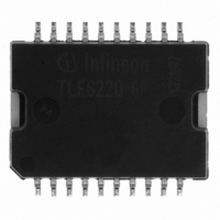
Manufacturer Part Number
TLE6220GP
Description
IC SW SMART QUAD LOSIDE DSO-20
Manufacturer
Infineon Technologies
Type
Low Sider
Datasheet
1.TLE6220GP.pdf
(19 pages)
Specifications of TLE6220GP
Input Type
SPI
Number Of Outputs
4
On-state Resistance
320 mOhm
Current - Output / Channel
3A
Current - Peak Output
6A
Voltage - Supply
4.5 V ~ 5.5 V
Operating Temperature
-40°C ~ 150°C
Mounting Type
Surface Mount
Package / Case
DSO-20
Switch Type
Low Side
Power Switch Family
TLE6220GP
Input Voltage
-0.3 to 7V
Power Switch On Resistance
320mOhm
Output Current
3A
Mounting
Surface Mount
Supply Current
1mA
Package Type
DSO
Operating Temperature (min)
-40C
Operating Temperature (max)
150C
Operating Temperature Classification
Automotive
Pin Count
22
Power Dissipation
3W
Packages
PG-DSO-20
Thermal Class
Heatslug down
Id Nom
4 x 1 A
Channels
4.0
Comment
inductive and resistive loads (e.g. injectors)
Lead Free Status / RoHS Status
Lead free / RoHS Compliant
Other names
SP000011903
SP000308873
TLE6220GPINTR
TLE6220GPNT
TLE6220GPT
TLE6220GPT
TLE6220GPXT
SP000308873
TLE6220GPINTR
TLE6220GPNT
TLE6220GPT
TLE6220GPT
TLE6220GPXT
Available stocks
Company
Part Number
Manufacturer
Quantity
Price
Company:

Part Number:
TLE6220GP
Manufacturer:
INFINEON
Quantity:
7 154
Company:
Part Number:
TLE6220GP
Manufacturer:
INFINEON
Quantity:
703
Part Number:
TLE6220GP
Manufacturer:
INFINEON/英飞凌
Quantity:
20 000
Part Number:
TLE6220GPAUMA2
Manufacturer:
INFINEON/英飞凌
Quantity:
20 000


SCLK - Serial Clock. The system clock pin clocks the internal shift register of the TLE
6220 GP. The serial input (SI) accepts data into the input shift register on the falling edge of
SCLK while the serial output (SO) shifts diagnostic information out of the shift register on the
rising edge of serial clock. It is essential that the SCLK pin is in a logic low state whenever
chip select CS makes any transition.
SI - Serial Input. Serial data bits are shifted in at this pin, the most significant bit first. SI infor-
mation is read in on the falling edge of SCLK. Input data is latched in the shift register and
then transferred to the control buffer of the output stages.
The input data consists of one byte, made up of four control bits and four data bits. The con-
trol word is used to program the device, to operate it in a certain mode as well as providing
diagnostic information (see page 11). The four data bits contain the input information for the
four channels, and are high active.
SO - Serial Output. Diagnostic data bits are shifted out serially at this pin, the most significant
bit first. SO is in a high impedance state until the CS pin goes to a logic low state. New diag-
nostic data will appear at the SO pin following the rising edge of SCLK.
switches all outputs OFF. An internal pull-up structure is provided on chip. As long as the re-
set pin is low the device is in low quiescent current mode and the supply current is reduced to
typ. 20µA.
Output Stage Control
The four outputs of the TLE 6220 GP can either be controlled in parallel (IN1...IN4), or via the
Serial Peripheral Interface (SPI).
Parallel Control
A Boolean operation (either AND or OR) is performed on each of the parallel inputs and re-
spective SPI data bits, in order to determine the states of the respective outputs. The type of
Boolean operation performed is programmed via the serial interface.
The parallel inputs are high or low active depending on the PRG pin. If the parallel input pins
are not connected (independent of high or low activity) it is guaranteed that the outputs 1 to 4
are switched OFF. PRG pin itself is internally pulled up when it is not connected.
PRG - Program pin.
V2.2
RESET
- Reset pin. If the reset pin is in a logic low state, it clears the SPI shift register and
PRG = High (V
PRG = Low (GND): Parallel inputs Channel 1 to 4 are low active.
S
):
Page
Parallel inputs Channel 1 to 4 are high active
7
Data Sheet TLE 6220 GP
2009-11-18
Related parts for TLE6220GP
Image
Part Number
Description
Manufacturer
Datasheet
Request
R

Part Number:
Description:
Manufacturer:
Infineon Technologies AG
Datasheet:
Part Number:
Description:
Manufacturer:
Infineon Technologies AG
Datasheet:
Part Number:
Description:
Manufacturer:
Infineon Technologies AG
Datasheet:
Part Number:
Description:
Manufacturer:
Infineon Technologies AG
Datasheet:
Part Number:
Description:
Manufacturer:
Infineon Technologies AG
Datasheet:
Part Number:
Description:
Manufacturer:
Infineon Technologies AG
Datasheet:
Part Number:
Description:
Manufacturer:
Infineon Technologies AG
Datasheet:
Part Number:
Description:
16-bit microcontroller with 2x2 KByte RAM
Manufacturer:
Infineon Technologies AG
Datasheet:
Part Number:
Description:
NPN silicon RF transistor
Manufacturer:
Infineon Technologies AG
Datasheet:
Part Number:
Description:
NPN silicon RF transistor
Manufacturer:
Infineon Technologies AG
Datasheet:
Part Number:
Description:
NPN silicon RF transistor
Manufacturer:
Infineon Technologies AG
Datasheet:
Part Number:
Description:
NPN silicon RF transistor
Manufacturer:
Infineon Technologies AG
Datasheet:
Part Number:
Description:
Si-MMIC-amplifier in SIEGET 25-technologie
Manufacturer:
Infineon Technologies AG
Datasheet:
Part Number:
Description:
IGBT Power Module
Manufacturer:
Infineon Technologies AG
Datasheet:
Part Number:
Description:
IC for switching-mode power supplies
Manufacturer:
Infineon Technologies AG
Datasheet: