MLP1N06CL ON Semiconductor, MLP1N06CL Datasheet

MOSFET N-CH 1A 62V TO-220AB

MLP1N06CL

Manufacturer Part Number
MLP1N06CL
Description
MOSFET N-CH 1A 62V TO-220AB
Manufacturer
ON Semiconductor
Series
SMARTDISCRETES™r
Type
Low Sider
Datasheet

Specifications of MLP1N06CL

Input Type
Non-Inverting
Number Of Outputs
1
Operating Temperature
-50°C ~ 150°C
Mounting Type
Through Hole
Package / Case
TO-220-3 (Straight Leads)
Configuration
Single
Transistor Polarity
N-Channel
Resistance Drain-source Rds (on)
0.75 Ohms
Forward Transconductance Gfs (max / Min)
1.4 S
Drain-source Breakdown Voltage
59 V
Gate-source Breakdown Voltage
+/- 10 V
Continuous Drain Current
1 A
Power Dissipation
40 W
Maximum Operating Temperature
+ 150 C
Mounting Style
Through Hole
Minimum Operating Temperature
- 40 C
Lead Free Status / RoHS Status
Contains lead / RoHS non-compliant
Voltage - Supply
-
Current - Output / Channel
-
On-state Resistance
-
Current - Peak Output
-
Lead Free Status / Rohs Status
No

Available stocks

Company
Part Number
Manufacturer
Quantity
Price
Part Number:
MLP1N06CL
Manufacturer:
ON
Quantity:
12 500
Part Number:
MLP1N06CLG
Manufacturer:
XILINX
Quantity:
600
N–Channel TO–220
short circuit protection, an integral gate–to–source clamp for ESD
protection and gate–to–drain clamp for over–voltage protection. No
additional gate series resistance is required when interfacing to the
output of a MCU, but a 40 k gate pulldown resistor is recommended
to avoid a floating gate condition.
devices to be applied without use of external transient suppression
components. The gate–to–source clamp protects the MOSFET input
from electrostatic gate voltage stresses up to 2.0 kV. The gate–to–drain
clamp protects the MOSFET drain from drain avalanche stresses that
occur with inductive loads. This unique design provides voltage
clamping that is essentially independent of operating temperature.
November, 2000 – Rev. 2
MAXIMUM RATINGS
THERMAL CHARACTERISTICS
Drain–to–Source Voltage
Drain–to–Gate Voltage
Gate–to–Source Voltage – Continuous
Drain Current – Continuous
Drain Current
Total Power Dissipation
Electrostatic Discharge Voltage
Operating and Storage Junction
Thermal Resistance, Junction to Case
Thermal Resistance, Junction to
Maximum Lead Temperature for
These SMARTDISCRETES devices feature current limiting for
The internal gate–to–source and gate–to–drain clamps allow the
Stress Applied to the Device and Protects the Load From
Overvoltage
Microprocessors
Temperature Compensated Gate–to–Drain Clamp Limits Voltage
Integrated ESD Diode Protection
Controlled Switching Minimizes RFI
Low Threshold Voltage Enables Interfacing Power Loads to
Semiconductor Components Industries, LLC, 2000
(R GS = 1.0 M )
(Human Body Model)
Temperature Range
Ambient
Soldering Purposes, 1/8 from case
– Single Pulse
Rating
(T C = 25 C unless otherwise noted)
Preferred Device
Symbol
T J , T stg
V DGR
V DSS
V GS
ESD
I DM
P D
T L
I D
t
Self–limited
–50 to 150
Clamped
Clamped
Value
3.12
62.5
260
1.8
2.0
40
10
1
Watts
Unit
Vdc
Vdc
Vdc
Adc
C/W
kV
C
C
MLP1N06CL
Preferred devices are recommended choices for future use
and best overall value.
1
2
Device
3
62 VOLTS (Clamped)
L1N06CL
LL
Y
WW
ORDERING INFORMATION
R DS(on) = 750 m
4
http://onsemi.com
CASE 221A
TO–220AB
1 AMPERE
STYLE 5
TO–220AB
Package
N–Channel
Publication Order Number:
MARKING DIAGRAM
= Device Code
= Location Code
= Year
= Work Week
& PIN ASSIGNMENT
Gate
1
L1N06CL
LLYWW
Drain
Drain
50 Units/Rail
MLP1N06CL/D
2
4
Shipping
3
Source

Related parts for MLP1N06CL

MLP1N06CL Summary of contents

Page 1

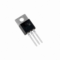
... VOLTS (Clamped) R DS(on) = 750 m N–Channel MARKING DIAGRAM & PIN ASSIGNMENT 4 4 Drain TO–220AB CASE 221A STYLE 5 L1N06CL LLYWW Gate 2 Drain L1N06CL = Device Code LL = Location Code Y = Year WW = Work Week ORDERING INFORMATION Device Package Shipping TO–220AB 50 Units/Rail Publication Order Number: MLP1N06CL/D 3 Source ...

Page 2

... Static Drain Current Limit ( 5 5 150 C) RESISTIVE SWITCHING CHARACTERISTICS (Note 1.) Turn–On Delay Time Rise Time ( 1 5 Ohms) Turn–Off Delay Time Fall Time 1. Indicates Pulse Test: Pulse Width 300 s, Duty Cycle MLP1N06CL Symbol unless otherwise noted) Symbol V (BR)DSS I DSS I GSS V GS(th) R DS(on D(lim) ...

Page 3

... Even with no heatsink, the MLP1N06CL can withstand a shorted load powered by an automotive battery ( Volts) for almost a second if its initial operating temperature is under 100 C. For longer periods of operation in the current– ...

Page 4

... Figure 3. I D(lim) Variation With Temperature Figure 5. On–Resistance Variation With Figure 6. Single Pulse Avalanche Energy versus Junction Temperature MLP1N06CL Figure 4. R DS(on) Variation With Gate–To–Source Voltage Temperature Figure 7. Drain–Source Sustaining Voltage Variation With Temperature http://onsemi.com 4 ...

Page 5

... Thermal Resistance – General Data and Its Use” provides detailed instructions. MAXIMUM DC VOLTAGE CONSIDERATIONS The maximum drain–to–source voltage that can be continuously applied across the MLP1N06CL when current limit is a function of the power that must be dissipated. This power is determined by the maximum current limit at maximum rated operating temperature MLP1N06CL (1 ...

Page 6

... To achieve high gate–to–drain clamp voltages, several voltage elements are strung together; the MLP1N06CL uses 8 such elements. Customarily, two voltage elements are used to provide a 14.4 volt gate–to–source voltage clamp. For the ...

Page 7

... PACKAGE DIMENSIONS MLP1N06CL TO–220 THREE–LEAD TO–220AB CASE 221A–09 ISSUE AA –T– http://onsemi.com 7 ...

Page 8

... Email: ONlit–asia@hibbertco.com JAPAN: ON Semiconductor, Japan Customer Focus Center 4–32–1 Nishi–Gotanda, Shinagawa–ku, Tokyo, Japan 141–0031 Phone: 81–3–5740–2700 Email: r14525@onsemi.com ON Semiconductor Website: http://onsemi.com For additional information, please contact your local Sales Representative. http://onsemi.com 8 MLP1N06CL/D ...

Related keywords