MLP1N06CL ON Semiconductor, MLP1N06CL Datasheet - Page 5
MLP1N06CL
Manufacturer Part Number
MLP1N06CL
Description
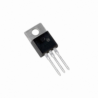
MOSFET N-CH 1A 62V TO-220AB
Manufacturer
ON Semiconductor
Series
SMARTDISCRETES™r
Type
Low Sider
Datasheet
1.MLP1N06CL.pdf
(8 pages)
Specifications of MLP1N06CL
Input Type
Non-Inverting
Number Of Outputs
1
Operating Temperature
-50°C ~ 150°C
Mounting Type
Through Hole
Package / Case
TO-220-3 (Straight Leads)
Configuration
Single
Transistor Polarity
N-Channel
Resistance Drain-source Rds (on)
0.75 Ohms
Forward Transconductance Gfs (max / Min)
1.4 S
Drain-source Breakdown Voltage
59 V
Gate-source Breakdown Voltage
+/- 10 V
Continuous Drain Current
1 A
Power Dissipation
40 W
Maximum Operating Temperature
+ 150 C
Mounting Style
Through Hole
Minimum Operating Temperature
- 40 C
Lead Free Status / RoHS Status
Contains lead / RoHS non-compliant
Voltage - Supply
-
Current - Output / Channel
-
On-state Resistance
-
Current - Peak Output
-
Lead Free Status / Rohs Status
No
Available stocks
Company
Part Number
Manufacturer
Quantity
Price
Company:

Part Number:
MLP1N06CL
Manufacturer:
ON
Quantity:
12 500
Company:
Part Number:
MLP1N06CLG
Manufacturer:
XILINX
Quantity:
600


FORWARD BIASED SAFE OPERATING AREA
voltage and drain current that a device can safely handle
when it is forward biased, or when it is on, or being turned
on. Because these curves include the limitations of
simultaneous high voltage and high current, up to the rating
of the device, they are especially useful to designers of linear
systems. The curves are based on a case temperature of 25 C
and a maximum junction temperature of 150 C. Limitations
for repetitive pulses at various case temperatures can be
determined by using the thermal response curves. ON
Semiconductor Application Note, AN569, “Transient
Thermal Resistance – General Data and Its Use” provides
detailed instructions.
MAXIMUM DC VOLTAGE CONSIDERATIONS
continuously applied across the MLP1N06CL when it is in
current limit is a function of the power that must be
dissipated. This power is determined by the maximum
current limit at maximum rated operating temperature
The FBSOA curves define the maximum drain–to–source
The maximum drain–to–source voltage that can be
Figure 9. Thermal Response (MLP1N06CL)
Figure 8. Maximum Rated Forward Bias
Safe Operating Area (MLP1N06CL)
http://onsemi.com
MLP1N06CL
5
(1.8 A at 150 C) and not the R DS(on) . The maximum voltage
can be calculated by the following equation:
where the value of R CA is determined by the heatsink that
is being used in the application.
DUTY CYCLE OPERATION
drain voltage can be increased. The maximum operating
temperature is related to the duty cycle (DC) by the
following equation:
duty cycle mode can be approximated by:
When operating in the duty cycle mode, the maximum
The maximum value of V DS applied when operating in a
V supply =
T C = (V DS x I D x DC x R CA ) + T A
V DS =
I D(lim) (R JC + R CA )
I D(lim) x DC x R JC
(150 – T A )
150 – T C
Related parts for MLP1N06CL
Image
Part Number
Description
Manufacturer
Datasheet
Request
R

Part Number:
Description:
ON Semiconductor [VOLTAGE REGULATOR]
Manufacturer:
ON Semiconductor
Datasheet:
Part Number:
Description:
357-036-542-201 CARDEDGE 36POS DL .156 BLK LOPRO
Manufacturer:
ON Semiconductor
Datasheet:
Part Number:
Description:
357-036-542-201 CARDEDGE 36POS DL .156 BLK LOPRO
Manufacturer:
ON Semiconductor
Datasheet:
Part Number:
Description:
357-036-542-201 CARDEDGE 36POS DL .156 BLK LOPRO
Manufacturer:
ON Semiconductor
Datasheet:
Part Number:
Description:
357-036-542-201 CARDEDGE 36POS DL .156 BLK LOPRO
Manufacturer:
ON Semiconductor
Datasheet:
Part Number:
Description:
357-036-542-201 CARDEDGE 36POS DL .156 BLK LOPRO
Manufacturer:
ON Semiconductor
Datasheet:
Part Number:
Description:
357-036-542-201 CARDEDGE 36POS DL .156 BLK LOPRO
Manufacturer:
ON Semiconductor
Datasheet:
Part Number:
Description:
357-036-542-201 CARDEDGE 36POS DL .156 BLK LOPRO
Manufacturer:
ON Semiconductor
Datasheet:
Part Number:
Description:
357-036-542-201 CARDEDGE 36POS DL .156 BLK LOPRO
Manufacturer:
ON Semiconductor
Datasheet:
Part Number:
Description:
357-036-542-201 CARDEDGE 36POS DL .156 BLK LOPRO
Manufacturer:
ON Semiconductor
Datasheet:
Part Number:
Description:
357-036-542-201 CARDEDGE 36POS DL .156 BLK LOPRO
Manufacturer:
ON Semiconductor
Datasheet:
Part Number:
Description:
Manufacturer:
ON Semiconductor
Datasheet:
Part Number:
Description:
Manufacturer:
ON Semiconductor
Datasheet:
Part Number:
Description:
Manufacturer:
ON Semiconductor
Datasheet: