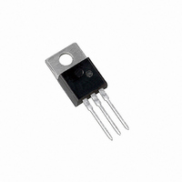
MLP1N06CL ON Semiconductor, MLP1N06CL Datasheet - Page 6

MLP1N06CL
Manufacturer Part Number
MLP1N06CL
Description
MOSFET N-CH 1A 62V TO-220AB
Manufacturer
ON Semiconductor
Series
SMARTDISCRETES™r
Type
Low Sider
Datasheet
1.MLP1N06CL.pdf
(8 pages)
Specifications of MLP1N06CL
Input Type
Non-Inverting
Number Of Outputs
1
Operating Temperature
-50°C ~ 150°C
Mounting Type
Through Hole
Package / Case
TO-220-3 (Straight Leads)
Configuration
Single
Transistor Polarity
N-Channel
Resistance Drain-source Rds (on)
0.75 Ohms
Forward Transconductance Gfs (max / Min)
1.4 S
Drain-source Breakdown Voltage
59 V
Gate-source Breakdown Voltage
+/- 10 V
Continuous Drain Current
1 A
Power Dissipation
40 W
Maximum Operating Temperature
+ 150 C
Mounting Style
Through Hole
Minimum Operating Temperature
- 40 C
Lead Free Status / RoHS Status
Contains lead / RoHS non-compliant
Voltage - Supply
-
Current - Output / Channel
-
On-state Resistance
-
Current - Peak Output
-
Lead Free Status / Rohs Status
No
Available stocks
Company
Part Number
Manufacturer
Quantity
Price
Company:
Part Number:
MLP1N06CL
Manufacturer:
ON
Quantity:
12 500
Company:
Part Number:
MLP1N06CLG
Manufacturer:
XILINX
Quantity:
600
ACTIVE CLAMPING
realization of the popular gate–to–source and gate–to–drain
Zener diode clamp elements. Until recently, such features
have been implemented only with discrete components
which consume board space and add system cost. The
SMARTDISCRETES technology approach economically
melds these features and the power chip with only a slight
increase in chip area.
polysilicon region monolithicly integrated with, but
electrically isolated from, the main device structure. Each
back–to–back diode element provides a temperature
compensated voltage element of about 7.2 volts. As the
polysilicon region is formed on top of silicon dioxide, the
diode elements are free from direct interaction with the
conduction regions of the power device, thus eliminating
parasitic electrical effects while maintaining excellent
thermal coupling.
voltage elements are strung together; the MLP1N06CL uses
8 such elements. Customarily, two voltage elements are used
to provide a 14.4 volt gate–to–source voltage clamp. For the
interface to the output of a microcontrol unit to control an
isolated load. No additional series gate resistance is
required, but a 40 k
recommended to avoid a floating gate condition in the event
of an MCU failure. The internal clamps allow the device to
be used without any external transistent suppressing
components.
SMARTDISCRETES technology can provide on–chip
In practice, back–to–back diode elements are formed in a
To achieve high gate–to–drain clamp voltages, several
The MLP1N06CL has been designed to allow direct
Figure 10. Switching Test Circuit
TYPICAL APPLICATIONS: INJECTOR DRIVER, SOLENOIDS, LAMPS, RELAY COILS
gate pulldown resistor is
http://onsemi.com
MLP1N06CL
6
MLP1N06CL, the integrated gate–to–source voltage
elements provide greater than 2.0 kV electrostatic voltage
protection.
is set less than that of the power MOSFET device. As soon
as the drain–to–source voltage exceeds this avalanche
voltage, the resulting gate–to–drain Zener current builds a
gate voltage across the gate–to–source impedance, turning
on the power device which then conducts the current. Since
virtually all of the current is carried by the power device, the
gate–to–drain voltage clamp element may be small in size.
This technique of establishing a temperature compensated
drain–to–source sustaining voltage (Figure 7) effectively
removes the possibility of drain–to–source avalanche in the
power device.
useful for snubbing loads where the inductive energy would
otherwise avalanche the power device. An improvement in
ruggedness of at least four times has been observed when
inductive energy is dissipated in the gate–to–drain clamped
conduction mode rather than in the more stressful
gate–to–source avalanche mode.
The avalanche voltage of the gate–to–drain voltage clamp
The gate–to–drain voltage clamp technique is particularly
Figure 11. Switching Waveforms


