AMIS30624C6245RG ON Semiconductor, AMIS30624C6245RG Datasheet - Page 55
AMIS30624C6245RG
Manufacturer Part Number
AMIS30624C6245RG
Description
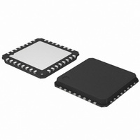
IC STEPPER DVR I2C 800MA 32-NQFP
Manufacturer
ON Semiconductor
Type
I2C Micro Stepping Motor Driverr
Datasheet
1.AMIS30624C6244RG.pdf
(56 pages)
Specifications of AMIS30624C6245RG
Applications
Stepper Motor Driver, 2 Phase
Number Of Outputs
1
Current - Output
800mA
Voltage - Supply
8 V ~ 29 V
Operating Temperature
-40°C ~ 165°C
Mounting Type
Surface Mount
Package / Case
32-VSQFP
Product
Stepper Motor Controllers / Drivers
Operating Supply Voltage
8 V to 29 V
Supply Current
800 mA
Mounting Style
SMD/SMT
Lead Free Status / RoHS Status
Lead free / RoHS Compliant
Voltage - Load
-
Lead Free Status / Rohs Status
Lead free / RoHS Compliant
Other names
766-1002-2
Available stocks
Company
Part Number
Manufacturer
Quantity
Price
Company:

Part Number:
AMIS30624C6245RG
Manufacturer:
ON Semiconductor
Quantity:
212
Company:
Part Number:
AMIS30624C6245RG
Manufacturer:
ON Semiconductor
Quantity:
1 850
Company:
Part Number:
AMIS30624C6245RG
Manufacturer:
ON Semiconductor
Quantity:
10 000


AMIS-30624
19.0 Soldering
19.1 Introduction to Soldering Surface Mount Packages
This text gives a very brief insight to a complex technology. A more in-depth account of soldering ICs can be found in the ON
Semiconductor “Data Handbook IC26; Integrated Circuit Packages” (document order number 9398 652 90011). There is no soldering
method that is ideal for all surface mount IC packages. Wave soldering is not always suitable for surface mount ICs, or for printed-
circuit boards with high population densities. In these situations re-flow soldering is often used.
19.2 Re-flow Soldering
Re-flow soldering requires solder paste (a suspension of fine solder particles, flux and binding agent) to be applied to the PCB by
screen printing, stencilling or pressure-syringe dispensing before package placement. Several methods exist for reflowing; for example,
infrared/convection heating in a conveyor type oven.
Throughput times (preheating, soldering and cooling) vary between 100 and 200 seconds depending on the heating method. Typical re-
flow peak temperatures range from 215 to 260°C. The top-surface temperature of the packages should preferably be kept below 230°C.
19.3 Wave Soldering
Conventional single wave soldering is not recommended for surface mount devices (SMDs) or PCBs with a high component density, as
solder bridging and non-wetting can present major problems. To overcome these problems, the double-wave soldering method was
specifically developed.
If wave soldering is used the following conditions must be observed for optimal results:
During placement and before soldering, the package must be fixed with a droplet of adhesive. The adhesive can be applied by screen
printing, pin transfer or syringe dispensing. The package can be soldered after the adhesive is cured. Typical dwell time is four seconds
at 250°C. A mildly-activated flux will eliminate the need for removal of corrosive residues in most applications.
19.4 Manual Soldering
Fix the component by first soldering two diagonally-opposite end leads. Use a low voltage (24V or less) soldering iron applied to the flat
part of the lead. Contact time must be limited to 10 seconds at up to 300°C.
When using a dedicated tool, all other leads can be soldered in one operation within two to five seconds between 270 and 320°C.
Table 35: Soldering Process
Package
BGA, SQFP
HLQFP, HSQFP, HSOP, HTSSOP, SMS
PLCC (3) , SO, SOJ
LQFP, QFP, TQFP
SSOP, TSSOP, VSO
Notes:
• Use a double-wave soldering method comprising a turbulent wave with high upward pressure followed by a smooth laminar wave.
• For packages with leads on two sides and a pitch (e):
• For packages with leads on four sides, the footprint must be placed at a 45º angle to the transport direction of the PCB. The
(1)
(2)
(3)
(4)
(5)
footprint must incorporate solder thieves downstream and at the side corners.
o
o
All surface mount (SMD) packages are moisture sensitive. Depending upon the moisture content, the maximum temperature (with respect to time) and body size
of the package, there is a risk that internal or external package cracks may occur due to vaporization of the moisture in them (the so called popcorn effect). For
details, refer to the drypack information in the “Data Handbook IC26; Integrated Circuit Packages; Section: Packing Methods.”
These packages are not suitable for wave soldering as a solder joint between the printed-circuit board and heatsink (at bottom version) can not be achieved, and
as solder may stick to the heatsink (on top version).
If wave soldering is considered, then the package must be placed at a 45° angle to the solder wave direction. The package footprint must incorporate solder
thieves downstream and at the side corners.
Wave soldering is only suitable for LQFP, TQFP and QFP packages with a pitch (e) equal to or larger than 0.8mm; it is definitely not suitable for packages with a
pitch (e) equal to or smaller than 0.65mm.
Wave soldering is only suitable for SSOP and TSSOP packages with a pitch (e) equal to or larger than 0.65mm; it is definitely not suitable for packages with a
pitch (e) equal to or smaller than 0.5mm.
Larger than or equal to 1.27mm, the footprint longitudinal axis is preferred to be parallel to the transport direction of the
PCB;
Smaller than 1.27mm, the footprint longitudinal axis must be parallel to the transport direction of the PCB. The footprint
must incorporate solder thieves at the downstream end.
Rev. 4 | Page 55 of 56 | www.onsemi.com
Not recommended
Not recommended
Not suitable
Not suitable
Suitable
Wave
(2)
(3)(4)
(5)
Soldering Method
Re-flow
Suitable
Suitable
Suitable
Suitable
Suitable
(1)
Related parts for AMIS30624C6245RG
Image
Part Number
Description
Manufacturer
Datasheet
Request
R

Part Number:
Description:
ON Semiconductor [VOLTAGE REGULATOR]
Manufacturer:
ON Semiconductor
Datasheet:
Part Number:
Description:
357-036-542-201 CARDEDGE 36POS DL .156 BLK LOPRO
Manufacturer:
ON Semiconductor
Datasheet:
Part Number:
Description:
357-036-542-201 CARDEDGE 36POS DL .156 BLK LOPRO
Manufacturer:
ON Semiconductor
Datasheet:
Part Number:
Description:
357-036-542-201 CARDEDGE 36POS DL .156 BLK LOPRO
Manufacturer:
ON Semiconductor
Datasheet:
Part Number:
Description:
357-036-542-201 CARDEDGE 36POS DL .156 BLK LOPRO
Manufacturer:
ON Semiconductor
Datasheet:
Part Number:
Description:
357-036-542-201 CARDEDGE 36POS DL .156 BLK LOPRO
Manufacturer:
ON Semiconductor
Datasheet:
Part Number:
Description:
357-036-542-201 CARDEDGE 36POS DL .156 BLK LOPRO
Manufacturer:
ON Semiconductor
Datasheet:
Part Number:
Description:
357-036-542-201 CARDEDGE 36POS DL .156 BLK LOPRO
Manufacturer:
ON Semiconductor
Datasheet:
Part Number:
Description:
357-036-542-201 CARDEDGE 36POS DL .156 BLK LOPRO
Manufacturer:
ON Semiconductor
Datasheet:
Part Number:
Description:
357-036-542-201 CARDEDGE 36POS DL .156 BLK LOPRO
Manufacturer:
ON Semiconductor
Datasheet:
Part Number:
Description:
357-036-542-201 CARDEDGE 36POS DL .156 BLK LOPRO
Manufacturer:
ON Semiconductor
Datasheet:
Part Number:
Description:
Manufacturer:
ON Semiconductor
Datasheet:
Part Number:
Description:
Manufacturer:
ON Semiconductor
Datasheet:
Part Number:
Description:
Manufacturer:
ON Semiconductor
Datasheet: