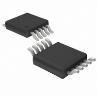
LT4351IMS Linear Technology, LT4351IMS Datasheet - Page 11

LT4351IMS
Manufacturer Part Number
LT4351IMS
Description
IC CTRLR MOSFET DIODE-OR 10MSOP
Manufacturer
Linear Technology
Datasheet
1.LT4351IMSPBF.pdf
(20 pages)
Specifications of LT4351IMS
Applications
Paralleled/Redundant Power Supplies
Fet Type
N-Channel
Number Of Outputs
1
Internal Switch(s)
No
Delay Time - Off
600ns
Voltage - Supply
1.2 V ~ 18 V
Current - Supply
1.4mA
Operating Temperature
-40°C ~ 85°C
Mounting Type
Surface Mount
Package / Case
10-MSOP, Micro10™, 10-uMAX, 10-uSOP
Lead Free Status / RoHS Status
Contains lead / RoHS non-compliant
Delay Time - On
-
Available stocks
Company
Part Number
Manufacturer
Quantity
Price
Part Number:
LT4351IMS
Manufacturer:
LT/凌特
Quantity:
20 000
Part Number:
LT4351IMS#PBF
Manufacturer:
LINEAR/凌特
Quantity:
20 000
APPLICATIONS INFORMATION
For V
Note that V
A first order approximation of the input current is:
Under normal operation, the V
and the boost regulator operates in Burst Mode
If any additional load is added, ensure that the regulator is
capable of supplying that load. As the load is increased,
the boost regulator will switch into continuous mode op-
eration. Further increases in load will collapse the boost
regulator voltage.
Operating the regulator with increased load will cause
increased IC power dissipation and temperature, which
must be taken into consideration.
A 100ns delay from detecting the switch current limit to
turning off the power switch produces an overshoot of the
inductor current from the 0.45A switch limit. The amount
of overshoot depends on the boost regulator inductance.
Choosing an inductor that can handle 0.75A peak current
will be sufficient for the recommended inductors.
Diode Selection
Schottky diodes, with their low forward voltage drop and
fast switching speed, are the best match for the LT4351
boost regulator. Select a diode that can handle 0.75A peak
current and a reverse breakdown of 15V greater than the
maximum V
I
VINVDD
IN
less than 2V, choose a DC resistance less than 0.2Ω.
200mV
Figure 7a. Example of Input Voltage Ringing
with Low C
V
DD
IN
= 1+
IN
current referred to the input supply is higher.
.
10.6
IN
V
IN
Capacitor at MOSFET Turn Off
•
10µs/DIV
I
80%
VDD
DD
current is under 10mA
4351 F07a
®
operation.
V
Low ESR (Equivalent Series Resistance) capacitors should
be used on V
Multilayer ceramic capacitors are the best choice, as
they have a very low ESR and are available in very small
packages. Always use a capacitor with a voltage rating at
least 12V greater than V
Capacitors
Two types of input capacitors are generally needed for the
LT4351. The first is a large bulk capacitor that takes care
of ringing associated with inductance of the input supply
lines and provides charge for the load when switching the
MOSFET. The input parasitic inductance in conjunction with
C
be stimulated by the boost regulator switch current or load
current transients when the MOSFETs are on. To reduce
ringing associated with input inductance, C
where C
ESR and L
While damped ringing is not necessarily bad, it may pro-
duce unexpected results as the LT4351 ideal diode reacts
to the varying V
or tantalum low ESR capacitor would be used. Figure 7a
illustrates V
it with a correctly sized value.
DD
B
C
and its ESR create an LCR network. The input LCR can
B
Capacitor Selection
200mV
≥
V
IN
B
Figure 7b. Example of Input Voltage with
Sufficient C
4 • L
is the capacitor value, R
R
IN
IN
ESR
2
is the inductance of the input lines.
IN
DD
for a low value of C
IN
to minimize the output ripple voltage.
to OUT voltage. Typically an electrolytic
IN
Capacitor at MOSFET Turn Off
IN
10µs/DIV
.
B
ESR
and Figure 7b shows
is the capacitor’s
4351 F07b
LT4351
B
should be:
11
4351fc


