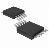
LT4351IMS Linear Technology, LT4351IMS Datasheet - Page 14

LT4351IMS
Manufacturer Part Number
LT4351IMS
Description
IC CTRLR MOSFET DIODE-OR 10MSOP
Manufacturer
Linear Technology
Datasheet
1.LT4351IMSPBF.pdf
(20 pages)
Specifications of LT4351IMS
Applications
Paralleled/Redundant Power Supplies
Fet Type
N-Channel
Number Of Outputs
1
Internal Switch(s)
No
Delay Time - Off
600ns
Voltage - Supply
1.2 V ~ 18 V
Current - Supply
1.4mA
Operating Temperature
-40°C ~ 85°C
Mounting Type
Surface Mount
Package / Case
10-MSOP, Micro10™, 10-uMAX, 10-uSOP
Lead Free Status / RoHS Status
Contains lead / RoHS non-compliant
Delay Time - On
-
Available stocks
Company
Part Number
Manufacturer
Quantity
Price
Part Number:
LT4351IMS
Manufacturer:
LT/凌特
Quantity:
20 000
Part Number:
LT4351IMS#PBF
Manufacturer:
LINEAR/凌特
Quantity:
20 000
Start-Up Considerations
There is no inherent shutdown in the part. As V
up, the boost regulator starts at about 0.85V and becomes
fully operational by 1.1V. The undervoltage and overvolt-
age comparators become accurate by 1.2V. The gate drive
amplifier keeps GATE low during this period with either
a passive pull-down, a weak active pull-down if OUT is
greater than 0.8V or with the full gate drive sink if V
above 2.2V.
LT4351
ORing Disparate Supplies
The LT4351 provides an easy solution for connecting
together different types of power sources. Again, because
of the low forward drop, the efficiency of the system is
improved and the voltage transition between supplies is
more accurate. In addition, the undervoltage and overvolt-
age features of the LT4351 provide options for enabling
and disabling the supplies that are not available from a
common diode. Figure 10 shows some examples of con-
necting disparate supplies.
APPLICATIONS INFORMATION
14
Isolated System Supply
ADAPTER
SYSTEM
SUPPLY
from Wall Adapter
WALL
BATTERY
ADAPTER
WALL
Three Source ORing Provides Protection
+
LT4351
Against Out of Range Supplies
LT4351
LOAD
Figure 10
LT4351
Isolated Battery Backup
BATTERY
ADAPTER
LOAD
WALL
+
LT4351
LT4351
SYSTEM
SUPPLY
IN
4351 F10
ramps
DD
LOAD
is
Once V
operates normally. The UV and OV pins will control the
enabling of the gate driver and once enabled, the V
OUT voltage controls MOSFET turn on.
If V
on the MOSFET, the GATE pin tracks with the V
crease until it reaches either the gate clamp voltage or
the compliance of the gate driver. If V
out V
Power Dissipation
The internal power dissipation of the LT4351 is comprised
of the following four major components: DC power dis-
sipation from V
dissipation in the boost switch including the base drive, and
dynamic power dissipation due to current used to charge
and discharge the MOSFETs. The DC components are:
Figure 11 shows the internal dissipation of the boost
regulator as a function of V
11 represents the worst-case condition with the regulator
on all the time, which does not occur in normal practice.
P
P
DD
DCVIN
DCVDD
IN
IN
is still being charged when the gate driver turns
or OUT, the GATE pin actively sinks low.
is greater than 1.2V and V
= I
0.30
0.25
0.20
0.15
0.10
= I
VIN
VDD
0
IN
• V
• V
, DC power dissipation from V
Figure 11. P
IN
DD
5
V
IN
IN
10
(V)
BOOST(MAX)
L = 10µH
and inductor value. Figure
DD
15
L = 4.7µH
DD
is up, the part then
is present with-
4351 F11
20
DD
DD
, the
IN
4351fc
in-
to


