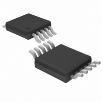
LT4351IMS Linear Technology, LT4351IMS Datasheet - Page 16

LT4351IMS
Manufacturer Part Number
LT4351IMS
Description
IC CTRLR MOSFET DIODE-OR 10MSOP
Manufacturer
Linear Technology
Datasheet
1.LT4351IMSPBF.pdf
(20 pages)
Specifications of LT4351IMS
Applications
Paralleled/Redundant Power Supplies
Fet Type
N-Channel
Number Of Outputs
1
Internal Switch(s)
No
Delay Time - Off
600ns
Voltage - Supply
1.2 V ~ 18 V
Current - Supply
1.4mA
Operating Temperature
-40°C ~ 85°C
Mounting Type
Surface Mount
Package / Case
10-MSOP, Micro10™, 10-uMAX, 10-uSOP
Lead Free Status / RoHS Status
Contains lead / RoHS non-compliant
Delay Time - On
-
Available stocks
Company
Part Number
Manufacturer
Quantity
Price
Part Number:
LT4351IMS
Manufacturer:
LT/凌特
Quantity:
20 000
Part Number:
LT4351IMS#PBF
Manufacturer:
LINEAR/凌特
Quantity:
20 000
LT4351
Design Example
The following demonstrates the calculations involved for
setting design components for a 5V system that requires
5A. Two supplies are used to do this. The V
be deemed in spec when it is within ±5% of nominal. Allow
5% of hysteresis for UV.
So,
Two separate resistive dividers are used.
For the UV divider:
The OV resistors are set as a straight resistive divider.
If the current in the R
R
APPLICATIONS INFORMATION
16
then
B
UV
OV
R1 = 1.68k. The closest 1% value is 1.69k
R2 =
R1=
R
R
= 25.48, use 25.5k
B
A
FAULT
FAULT
=
=
UV
I
UV
UVHYST
200mA
OV
0.3V
FAULT
= 4.75V, UV
= 5.5
R2 • V
HYST
V
FAULT
OV
UV
=
– V
= 1.5k use 1.47k (1%)
10µF
V
5V
IN
0.25V
– 1
10µA
UV
A
, R
HYST
=
B
R
220µF
divider is 200µA, then:
4.75V – 0.3V
A
= 25k Use 24.9k
24.9k • 0.3V
= 0.25V
4.7µH
=
5.5
0.3
R
25.5k
1%
R
1.47k
1%
(
B
A
– 1
R2
24.9k
1%
R1
1.69k
1%
1.47k
IN
Figure 15. 5V/5A Design Example
supply will
)
1
10µF
MBR0530
MBR0530
0.1µF
For regulation, the MOSFETs must have:
This very low value cannot be accomplished with a single
set of MOSFETs so a decision must be made whether to
use multiple MOSFETs or to live with an unregulated off-
set. Since low mΩ R
a single MOSFET would still be acceptable. For R
= 4mΩ the drop is 2 • 5A • 4mΩ = 40mV. The finished
schematic is shown in Figure 15.
Layout Considerations
There are two considerations for board layout. The first
is that V
to the part as possible. The GND pin should represent the
common tie point. The resistive dividers for UV and OV
should tie here as well.
Take care that current flow to the load (both through V
and GND), does not inadvertently produce errors due to
IR drops in PCB traces.
Keep the traces to the MOSFETs wide and short and close
to the part. The PCB traces associated with the power path
through the MOSFETs should have low resistance.
1µF
R
7
6
4
2
DS
UV
OV
SW
V
V
DD
IN
3
<
IN
15mV
2 • 5A
and V
Si4838DY
LT4351
GATE
GND
1
5
DD
= 1.5mΩ
bypass capacitors should be as close
STATUS
DS(ON)
FAULT
OUT
10
9
8
is available, the IR drop using
4351 F15
10µF
2k
OUT
5V
2k
DS(ON)
4351fc
IN


