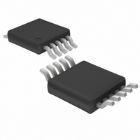
LT4351IMS Linear Technology, LT4351IMS Datasheet - Page 15

LT4351IMS
Manufacturer Part Number
LT4351IMS
Description
IC CTRLR MOSFET DIODE-OR 10MSOP
Manufacturer
Linear Technology
Datasheet
1.LT4351IMSPBF.pdf
(20 pages)
Specifications of LT4351IMS
Applications
Paralleled/Redundant Power Supplies
Fet Type
N-Channel
Number Of Outputs
1
Internal Switch(s)
No
Delay Time - Off
600ns
Voltage - Supply
1.2 V ~ 18 V
Current - Supply
1.4mA
Operating Temperature
-40°C ~ 85°C
Mounting Type
Surface Mount
Package / Case
10-MSOP, Micro10™, 10-uMAX, 10-uSOP
Lead Free Status / RoHS Status
Contains lead / RoHS non-compliant
Delay Time - On
-
Available stocks
Company
Part Number
Manufacturer
Quantity
Price
Part Number:
LT4351IMS
Manufacturer:
LT/凌特
Quantity:
20 000
Part Number:
LT4351IMS#PBF
Manufacturer:
LINEAR/凌特
Quantity:
20 000
APPLICATIONS INFORMATION
Since the boost regulator supplies current for V
current is the V
age current to charge the gate. For a gate charge of 50nC
at a 10kHz rate, this adds 0.5mA of current. The power
dissipated by the boost regulator to supply the 4mA is
shown in Figure 12, representing a more typical situation.
Finally, the gate driver dissipates power internally when
charging and discharging the gate of the MOSFETs. This
power depends on the input capacitance of the MOSFETs
and the frequency of charge and discharge. The power
associated with this can be approximated by:
where Q
to the clamp voltage (7.4V) and f
P
GATE
G
is the required gate charge to charge the MOSFET
0.025
0.015
0.010
0.005
0.020
= f
G
0
L = 4.7µH
• V
DD
DD
supply current (3.5mA) plus the aver-
Figure 12. P
5
• Q
G
• 1–
V
IN
10
(V)
BOOST(TYP)
G
V
is the frequency at which
16
IN
15
0.16
0.14
0.12
0.10
0.08
0.06
4351 F12
20
0
Figure 14. Total Power (Typical)
V
0.5mA GATE CURRENT
DD
L = 10µH
= V
DD
IN
5
+ 10
, the
L = 4.7µH
V
IN
10
(V)
the gate is charged and discharged. Normally f
the resulting power would be very low. Figure 13 shows
P
Total power dissipation is the sum of all of P
P
power dissipation of a typical application at steady state.
The die junction temperature is then computed as:
where T
ent temperature, θ
(120°C/W) and P
Therefore, a 0.1W power dissipation causes a 12° tem-
perature rise above ambient.
GATE
BOOST
T
J
15
= T
for a 50nC gate charge at a 1kHz rate.
and P
J
A
is the die junction temperature, T
0.004
0.003
0.002
0.001
+ θ
4351 F14
Figure 13. P
0
20
GATE
JA
0
f
Q
GATE
G
• P
= 50nC
. Figure 14 is representative of the total
TOTAL
JA
= 1kHz
TOTAL
5
is the thermal resistance of the part
GATE
is ascertained from the above.
vs V
V
IN
10
(V)
IN
(V
DD
15
= V
IN
+ 10.7)
4351 F13
DCVIN
A
LT4351
20
is the ambi-
G
is low and
, P
15
DCVDD
4351fc
,


