IR3523MTRPBF International Rectifier, IR3523MTRPBF Datasheet - Page 3
IR3523MTRPBF
Manufacturer Part Number
IR3523MTRPBF
Description
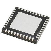
IC XPHASE3 CTLR VR11.1 40-MLPQ
Manufacturer
International Rectifier
Series
XPhase3™r
Datasheet
1.IR3523MTRPBF.pdf
(37 pages)
Specifications of IR3523MTRPBF
Applications
Processor
Current - Supply
10mA
Voltage - Supply
4.75 V ~ 7.5 V
Operating Temperature
0°C ~ 100°C
Mounting Type
Surface Mount
Package / Case
40-MLPQ
Ic Function
Dual Output Control IC
Supply Voltage Range
4.75V To 7.5V
Operating Temperature Range
0°C To +150°C
Digital Ic Case Style
MLPQ
No. Of Pins
40
Controller Type
XPhase
Rohs Compliant
Yes
Package
40-Lead MLPQ
Circuit
X-Phase Control IC
Switch Freq (khz)
250kHz to 1.5MHz
Pbf
PbF Option Available
Lead Free Status / RoHS Status
Lead free / RoHS Compliant


Page 3 of 37
PIN#
38, 39,
12
13
14
15
16
17
18
19
21
22
23
24
25
26
27
28
29
31
32
33
34
35
36
37
40
PIN SYMBOL
VID2_1, VID2_2
ROSC/OVP
VCCLDRV
VOSEN2+
VOSEN1+
VOSEN2-
VOSEN1-
SS/DEL1
PHSOUT
EAOUT1
OCSET1
CLKOUT
VCCLFB
VID2_0,
VOUT2
VOUT1
VDAC1
VDRP1
PHSIN
LGND
VCCL
PG1
PG2
FB2
FB1
IIN1
Output 2 Error Amplifier inverting input
Output 2 remote sense amplifier output.
Output 2 remote sense amplifier input. Connect to output at the load.
Output 2 remote sense amplifier input. Connect to ground at the load.
Output 1 remote sense amplifier input. Connect to ground at the load.
Output 1 remote sense amplifier input. Connect to output at the load.
Output 1 remote sense amplifier output.
Inverting input to the output 1 Error Amplifier
Output 1 error amplifier output
Programs the output 1 constant converter output current limit and hiccup over-
current threshold through an external resistor tied to VDAC1 and an internal
current source from this pin. Over-current protection can be disabled by
connecting a resistor from this pin to VDAC1 to program the threshold higher
than the possible signal into the IIN pin from the phase ICs but no greater than
5V (do not float this pin as improper operation will occur).
Output 1 reference voltage programmed by the VID inputs and error amplifier
non-inverting input. Connect an external RC network to LGND to program
dynamic VID slew rate and provide compensation for the internal buffer
amplifier.
Programs output 1 startup and over current protection delay timing. Connect an
external capacitor to LGND to program.
Output 1 average current input from the output 1 phase IC(s). This pin is also
used to communicate over voltage condition to phase ICs.
Output 1 Buffered IIN signal. Connect an external RC network to FB1 to
program converter output impedance.
Connect a resistor to LGND to program oscillator frequency and OCSET,
VDAC1 and VREF2 bias currents. Oscillator frequency equals switching
frequency per phase. The pin voltage is 0.6V during normal operation and
higher than 1.6V if over-voltage condition is detected.
Open collector output. Asserted when Output 1 is regulated.
Local Ground for internal circuitry and IC substrate connection.
Clock output at switching frequency multiplied by phase number. Connect to
CLKIN pins of phase ICs.
Phase clock output at switching frequency per phase. Connect to PHSIN pin of
the first phase IC.
Feedback input of phase clock. Connect to PHSOUT pin of the last phase IC.
Output of the voltage regulator, and power input for clock oscillator circuitry.
Connect a decoupling capacitor to LGND.
Non-inverting input of the voltage regulator error amplifier. Output voltage of the
regulator is programmed by the resistor divider connected to VCCL.
Output of the VCCL regulator error amplifier to control external transistor. The
pin senses the converter input voltage through a resistor.
Open collector output. Asserted when Output 2 output is regulated.
VID inputs for Output 2
PIN DESCRIPTION
June 20, 2008
IR3523
Related parts for IR3523MTRPBF
Image
Part Number
Description
Manufacturer
Datasheet
Request
R

Part Number:
Description:
SCHOTTKY RECTIFIER
Manufacturer:
International Rectifier Corp.
Datasheet:
Part Number:
Description:
SCHOTTKY RECTIFIER
Manufacturer:
International Rectifier Corp.
Datasheet:
Part Number:
Description:
SCHOTTKY RECTIFIER
Manufacturer:
International Rectifier Corp.
Datasheet:
Part Number:
Description:
SCHOTTKY RECTIFIER
Manufacturer:
International Rectifier Corp.
Datasheet:
Part Number:
Description:
SCHOTTKY RECTIFIER
Manufacturer:
International Rectifier Corp.
Datasheet:
Part Number:
Description:
SCHOTTKY RECTIFIER
Manufacturer:
International Rectifier Corp.
Datasheet:
Part Number:
Description:
SCHOTTKY RECTIFIER
Manufacturer:
International Rectifier Corp.
Datasheet:
Part Number:
Description:
SCHOTTKY RECTIFIER
Manufacturer:
International Rectifier Corp.
Datasheet:
Part Number:
Description:
SCHOTTKY RECTIFIER
Manufacturer:
International Rectifier Corp.
Datasheet:
Part Number:
Description:
SCHOTTKY RECTIFIER
Manufacturer:
International Rectifier Corp.
Datasheet:
Part Number:
Description:
SCHOTTKY RECTIFIER
Manufacturer:
International Rectifier Corp.
Datasheet:
Part Number:
Description:
SCHOTTKY RECTIFIER
Manufacturer:
International Rectifier Corp.
Datasheet:
Part Number:
Description:
SCHOTTKY RECTIFIER
Manufacturer:
International Rectifier Corp.
Datasheet:
Part Number:
Description:
SCHOTTKY RECTIFIER
Manufacturer:
International Rectifier Corp.
Datasheet:
Part Number:
Description:
SCHOTTKY RECTIFIER
Manufacturer:
International Rectifier Corp.
Datasheet: