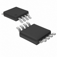
LTC1966CMS8#TRPBF Linear Technology, LTC1966CMS8#TRPBF Datasheet - Page 25

LTC1966CMS8#TRPBF
Manufacturer Part Number
LTC1966CMS8#TRPBF
Description
IC PREC RMS/DC CONV MCRPWR 8MSOP
Manufacturer
Linear Technology
Specifications of LTC1966CMS8#TRPBF
Current - Supply
155µA
Voltage - Supply
2.7 V ~ 5.5 V
Mounting Type
Surface Mount
Package / Case
8-MSOP, Micro8™, 8-uMAX, 8-uSOP,
Lead Free Status / RoHS Status
Lead free / RoHS Compliant
Available stocks
Company
Part Number
Manufacturer
Quantity
Price
applicaTions inForMaTion
The two 10MΩ resistors not connected to the supply can
be any value as long as they match and the feed voltage
is changed for 30nA injection. The op amp gain is only
1.00845, so the output is dominated by the LTC1966 RMS
results, which keeps errors low. With the values shown,
the resistors can be ±2% and only introduce ±170ppm of
gain error. The 84.5k resistor is the closest match in the
1% EIA values but if the 2% EIA value of 82k were used
instead, the gain would only be reduced by 248ppm.
This low error sensitivity is important because the LTC1966
output impedance is 85kΩ ±11.8%, which can create a
gain error of ±0.1%; enough to degrade the overall gain
accuracy somewhat. This gain variation term is increased
with lower value feed resistors, and decreased with higher
value feed resistors.
A bigger error caused by the variation of the LTC1966
output impedance is imperfect cancelation of the output
offset introduced by the injected current. The offset correc-
tion provided by the LT1494 will be based on a consistent
84.5kΩ times the injected current, while the LTC1966 output
impedance will vary enough that the output offset will have
a ±300µV range about the nominal 2.5mV. If this level of
output offset is not acceptable, either system calibration
or a potentiometer in the LT1494 feedback may be needed.
If the two 10MΩ feed resistors to the LT1494 have signifi-
cant mismatch, cancellation of the 2.5mV offset would be
further impacted, so it is probably worth paying an extra
penny or so for 1% resistors or even the better temperature
stability of thin film devices. The 300mV feed voltage is
not particularly critical because it is nominally cancelled,
but the offset errors due to these resistance mismatches
is scaled by that voltage.
Note that the input bias current of the op amp used in
Figure 23 is also nominally cancelled, but it will add or
subtract to the total current injected into the LTC1966
output. With the 1nA I
While it is possible to eliminate the feed resistors by using
an op amp with a PNP input stage whose I
BIAS
of the LT1494 this is negligible.
BIAS
is 30nA
or more, I
this circuit needs a minimum of 30nA, therefore such an
approach may not always work.
Because the circuit of Figure 23 subtracts the offset cre-
ated by the injected current, the LT1494 output with zero
LTC1966 input will rest at +2.5mV, nominal before offsets,
rather then the 5mV seen in Figure 22.
Output Errors Versus Frequency
As mentioned in the Design Cookbook, the LTC1966 per-
forms very well with low frequency and very low frequency
inputs, provided a large enough averaging capacitor is used.
However, the LTC1966 will have additional dynamic errors as
the input frequency is increased. The LTC1966 is designed
for high accuracy RMS-to-DC conversion of signals into
the audible range. The input sampling amplifiers have a
– 3dB frequency of 800kHz or so. However, the switched
capacitor circuitry samples the inputs at a modest 100kHz
nominal. The response versus frequency is depicted in the
Typical Performance Characteristics titled Input Signal
Bandwidth. Although there is a pattern to the response
versus frequency that repeats every sample frequency, the
errors are not overwhelming. This is because LTC1966 RMS
calculation is inherently wideband, operating properly with
minimal oversampling, or even undersampling, using sev-
eral proprietary techniques to exploit the fact that the RMS
value of an aliased signal is the same as the RMS value of
the original signal. However, a fundamental feature of the
∆S modulator is that sample estimation noise is shaped
such that minimal noise occurs with input frequencies
much less than the sampling frequency, but such noise
peaks when input frequency reaches half the sampling
frequency. Fortunately the LTC1966 output averaging filter
greatly reduces this error, but the RMS-to-DC topology
frequency shifts the noise to low (baseband) frequencies.
So with input frequencies above 5kHz to 10kHz, the output
will slowly wander around ±a few percent.
BIAS
is usually only specified for maximum and
LTC1966
25
1966fb


