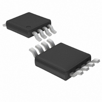
LTC1966CMS8#TRPBF Linear Technology, LTC1966CMS8#TRPBF Datasheet - Page 30

LTC1966CMS8#TRPBF
Manufacturer Part Number
LTC1966CMS8#TRPBF
Description
IC PREC RMS/DC CONV MCRPWR 8MSOP
Manufacturer
Linear Technology
Specifications of LTC1966CMS8#TRPBF
Current - Supply
155µA
Voltage - Supply
2.7 V ~ 5.5 V
Mounting Type
Surface Mount
Package / Case
8-MSOP, Micro8™, 8-uMAX, 8-uSOP,
Lead Free Status / RoHS Status
Lead free / RoHS Compliant
Available stocks
Company
Part Number
Manufacturer
Quantity
Price
applicaTions inForMaTion
LTC1966
Whatever calibration scheme is used, the linearity of the
LTC1966 will improve the calibrated accuracy over that
achievable with older log/antilog RMS-to-DC converters.
Additionally, calibration using DC reference voltages are
essentially as accurate with the LTC1966 as those using
AC reference voltages. Older log/antilog RMS-to-DC
converters required nonlinear input stages (rectifiers)
whose linearity would typically render DC based calibra-
tion unworkable.
The following are four suggested calibration methods.
Implementations of the suggested adjustments are de-
pendent on the system design, but in many cases, gain
and output offset can be corrected in the digital domain,
and will include the effect of all gains and offsets from the
LTC1966 output through the ADC. Input offset voltage, on
the other hand, will have to be corrected with adjustment
to the actual analog input to the LTC1966.
The methods below assume the unaltered linearity of the
LTC1966, i.e. without the monotonicity fix of Figure 21.
If this is present, the V
taken out before using either method for which V
not calibrated. Also, the nonlinearity it introduces will
increase the 20mV readings discussed below by 0.78%
but increase the 200mV readings only 78ppm. There
are a variety of ways to deal with these errors, including
possibly ignoring them, but the specifics will depend on
system requirements. Designers are cautioned to avoid
the temptation to digitally take out the hyperbolic transfer
function introduced because if the offsets are not exactly
the nominals assumed, the system will end up right back
where it began with a potential discontinuity with zero
input, either from a divide by zero or from a square root
of a negative number in the calculations to undo the hy-
perobic transfer function. An adaptive algorithm would
most likely be necessary to safely take out more than half
of the introduced nonlinearity.
If a 5V reference is used in the connection of Figure 25b,
the V
30
OOS
and nonlinearity created would be even larger,
OOS
shift it introduces should be
OOS
is
and will no doubt be more tempting to correct for. Design-
ers are likewise cautioned against correcting for all of the
nonlinearity.
AC-Only, 1 Point
The dominant error at full-scale will be caused by the
gain error, and by applying a full-scale sine wave input,
this error can be measured and corrected for. Unlike older
log/antilog RMS-to-DC converters, the correction should
be made for zero error at full scale to minimize errors
throughout the dynamic range.
The best frequency for the calibration signal is roughly ten
times the – 0.1% DC error frequency. For 1µF , –0.1% DC
error occurs at 8Hz, so 80Hz is a good calibration frequency,
although anywhere from 60Hz to 100Hz should suffice.
The trade-off here is that on the one hand, the DC error
is input frequency dependent, so a calibration signal
frequency high enough to make the DC error negligible
should be used. On the other hand, as low a frequency as
can be used is best to avoid attenuation of the calibrated
AC signal, either from parasitic RC loading or insufficient
op amp gain. For instance, with a 1kHz calibration signal,
a 1MHz op amp will typically only have 60dB of open loop
gain, so it could attenuate the calibration signal a full 0.1%.
AC-Only, 2 Point
The next most significant error for AC-coupled applications
will be the effect of output offset voltage, noticeable at the
bottom end of the input scale. This too can be calibrated
out if two measurements are made, one with a full-scale
sine wave input and a second with a sine wave input (of
the same frequency) at 10% of full-scale. The trade-off in
selecting this second level is that it should be small enough
that the gain error effect becomes small compared to the
gain error effect at full-scale, while on the other hand,
not using so small an input that the input offset voltage
becomes an issue.
1966fb


