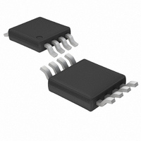
LTC1966CMS8#TRPBF Linear Technology, LTC1966CMS8#TRPBF Datasheet - Page 26

LTC1966CMS8#TRPBF
Manufacturer Part Number
LTC1966CMS8#TRPBF
Description
IC PREC RMS/DC CONV MCRPWR 8MSOP
Manufacturer
Linear Technology
Specifications of LTC1966CMS8#TRPBF
Current - Supply
155µA
Voltage - Supply
2.7 V ~ 5.5 V
Mounting Type
Surface Mount
Package / Case
8-MSOP, Micro8™, 8-uMAX, 8-uSOP,
Lead Free Status / RoHS Status
Lead free / RoHS Compliant
Available stocks
Company
Part Number
Manufacturer
Quantity
Price
applicaTions inForMaTion
This is a much higher accuracy than the LTC1966 conver-
sion limits, and far better than the accuracy computed via
the simplistic resistive divider model:
LTC1966
Input Impedance
The LTC1966 true RMS-to-DC converter utilizes a 2.5pF
capacitor to sample the input at a nominal 100kHz sample
frequency. This accounts for the 8MΩ input impedance.
See Figure 24 for the equivalent analog input circuit. Note
however, that the 8MΩ input impedance does not directly
affect the input sampling accuracy. For instance, if a 100k
source resistance is used to drive the LTC1966, the sampling
action of the input stage will drag down the voltage seen
at the input pins with small spikes at every sample clock
edge as the sample capacitor is connected to be charged.
The time constant of this combination is small, 2.5pF •
100kΩ = 250ns, and during the 2.5µs period devoted to
sampling, ten time constants elapse. This allows each
sample to settle to within 46ppm and it is these samples
that are used to compute the RMS value.
26
IN1
IN2
I
I
IN1
IN2
V
Figure 24. LTC1966 Equivalent Analog Input Circuit
IN
V
V
=
=
DD
SS
=
V
V
V
V
V
SOURCE
SOURCE
SOURCE
DD
SS
R
R
SW
SW
6k
6k
(TYP)
(TYP)
8
– . %
R
M
IN
1 25
+
8
+
R
M
R
IN
SOURCE
100
k
C
2.5pF
(TYP)
C
2.5pF
(TYP)
1966 F24
EQ
EQ
I IN
I IN
R
( )
( )
EQ
1
2
=
AVG
AVG
8
M
=
Ω
=
V
V
IN
IN
1
R
2
R
−
EQ
−
EQ
V
V
IN
IN
2
1
This resistive divider calculation does give the correct
model of what voltage is seen at the input terminals by a
parallel load averaged over a several clock cycles, which is
what a large shunt capacitor will do—average the current
spikes over several clock cycles.
When high source impedances are used, care must be taken
to minimize shunt capacitance at the LTC1966 input so as
not to increase the settling time. Shunt capacitance of just
2.5pF will double the input settling time constant and the
error in the above example grows from 46ppm to 0.67%
(6700ppm). A 13pF scope probe will increase the error
to almost 20%. As a consequence, it is important to not
try to filter the input with large input capacitances unless
driven by a low impedance. Keep time constant << 2.5µs.
When the LTC1966 is driven by op amp outputs, whose low
DC impedance can be compromised by sharp capacitive
load switching, a small series resistor may be added. A
10k resistor will easily settle with the 2.5pF input sampling
capacitor to within 1ppm.
These are important points to consider both during design
and debug. During lab debug, and even production testing,
a high value series resistor to any test point is advisable.
Output Impedance
The LTC1966 output impedance during operation is simi-
larly due to a switched capacitor action. In this case, 59pF
of on-chip capacitance operating at 100kHz translates into
170kΩ. The closed loop RMS-to-DC calculation cuts that
in half to the nominal 85kΩ specified.
In order to create a DC result, a large averaging capacitor
is required. Capacitive loading and time constants are not
an issue on the output.
1966fb


