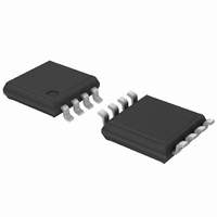
SE97PW,118 NXP Semiconductors, SE97PW,118 Datasheet - Page 20

SE97PW,118
Manufacturer Part Number
SE97PW,118
Description
IC TEMP SENSOR DIMM 8-TSSOP
Manufacturer
NXP Semiconductors
Datasheet
1.SE97TK118.pdf
(55 pages)
Specifications of SE97PW,118
Function
Temp Monitoring System (Sensor)
Topology
ADC (Sigma Delta), Comparator, Register Bank
Sensor Type
Internal
Sensing Temperature
-40°C ~ 125°C
Output Type
I²C™/SMBus™
Output Alarm
Yes
Output Fan
Yes
Voltage - Supply
3 V ~ 3.6 V
Operating Temperature
-40°C ~ 125°C
Mounting Type
Surface Mount
Package / Case
8-TSSOP
Temperature Threshold
+ 165 C
Full Temp Accuracy
1 %
Digital Output - Bus Interface
I2C, SMBus
Digital Output - Number Of Bits
11 bit
Supply Voltage (max)
3.6 V
Supply Voltage (min)
3 V
Description/function
Memory Module Temperature Sensor
Maximum Operating Temperature
+ 125 C
Minimum Operating Temperature
- 40 C
Supply Current
250 uA
Lead Free Status / RoHS Status
Lead free / RoHS Compliant
Other names
568-4291-2
935284062118
SE97PW-T
935284062118
SE97PW-T
NXP Semiconductors
Table 6.
Instructions with R/W bit = 0.
SE97_7
Product data sheet
Status
Permanently
protected
Protected with
RWP
Not protected
Fig 18. Software Write Protect (read)
(1) Refer to
SDA
X = Don’t Care
Acknowledge when writing data or defining write protection
7.10.2.1 Permanent Write Protection (PWP)
7.10.2.2 Reversible Write Protection (RWP) and Clear Reversible Write Protection (CRWP)
START condition
S
Table 7
0
PWP or RWP
Instruction
PWP, RWP or CRWP
page or byte write in
lower 128 bytes
RWP
CRWP
PWP
page or byte write in
lower 128 bytes
CRWP
page or byte write
slave address (memory)
1
If the software write-protection has been set with the PWP instruction, the first 128 bytes
of the memory are permanently write-protected. This write-protection cannot be cleared
by any instruction, or by power-cycling the device. Also, once the PWP instruction has
been successfully executed, the device no longer acknowledges any instruction (with 4-bit
fixed address of 0110b) to access the write-protection settings.
If the software write-protection has been set with the RWP instruction, it can be cleared
again with a CRWP instruction.
The two instructions, RWP and CRWP have the same format as a Byte Write instruction,
but with a different setting for the hardware address pins (as shown in
Byte Write instruction, it is followed by an address byte and a data byte, but in this case
the contents are all ‘Don’t Care’
must be applied on the A0 pin, and specific logical levels must be applied on the other two
(A1 and A2), as shown in
regarding the exact state of the acknowledge bit.
1
0
A2 A1 A0
R/W acknowledge
1
ACK
NACK
ACK
NACK
ACK
ACK
ACK
ACK
ACK
ACK
A
from slave
Rev. 07 — 29 January 2010
X
DDR memory module temp sensor with integrated SPD, 3.3 V
X
Table
dummy byte address
not significant
not significant
not significant
address
Address
address
not significant
not significant
address
not significant
X
(1)
X
5.
(Figure
X
no acknowledge
X
17). Another difference is that the voltage, V
from slave
X
NACK
ACK
NACK
ACK
ACK
ACK
ACK
ACK
ACK
ACK
X
(1)
A
X
Data byte
not significant
data
not significant
not significant
not significant
data
not significant
not significant
data
X
X
dummy data
X
X
no acknowledge
X
STOP condition
NACK
NACK
ACK
NACK
ACK
NACK
ACK
ACK
ACK
ACK
X
from slave
Table
© NXP B.V. 2010. All rights reserved.
X
002aac644
(1)
A
5). Like the
no
no
yes
no
Write cycle
(T
no
yes
yes
no
yes
P
SE97
cy(W)
20 of 55
)
I(ov)
,


