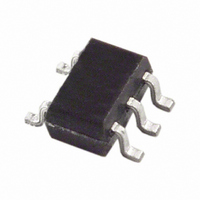
TMP05AKSZ-500RL7 Analog Devices Inc, TMP05AKSZ-500RL7 Datasheet - Page 5

TMP05AKSZ-500RL7
Manufacturer Part Number
TMP05AKSZ-500RL7
Description
IC PWM TEMP SNSR CMOS/TTL SC70-5
Manufacturer
Analog Devices Inc
Datasheet
1.TMP05ARTZ-500RL7.pdf
(28 pages)
Specifications of TMP05AKSZ-500RL7
Function
Temp Monitoring System (Sensor)
Topology
ADC (Sigma Delta), Averaging Control
Sensor Type
Internal
Sensing Temperature
-40°C ~ 150°C
Output Type
CMOS/TTL
Output Alarm
No
Output Fan
No
Voltage - Supply
3 V ~ 5.5 V
Operating Temperature
-40°C ~ 150°C
Mounting Type
Surface Mount
Package / Case
SC-70-5, SC-88A, SOT-323-5, SOT-353, 5-TSSOP
Ic Output Type
Digital
Sensing Accuracy Range
± 2°C
Supply Current
425µA
Supply Voltage Range
3V To 5.5V
Resolution (bits)
12bit
Sensor Case Style
SC-70
No. Of Pins
5
Temperature Sensor Function
Temp Sensor
Package Type
SC-70
Operating Temperature (min)
-40C
Operating Temperature (max)
150C
Operating Temperature Classification
Automotive
Operating Supply Voltage (min)
3V
Operating Supply Voltage (typ)
3.3/5V
Operating Supply Voltage (max)
5.5V
Accuracy
± 0.5
Rohs Compliant
Yes
Lead Free Status / RoHS Status
Lead free / RoHS Compliant
Lead Free Status / RoHS Status
Lead free / RoHS Compliant, Lead free / RoHS Compliant
Other names
TMP05AKSZ-500RL7TR
Available stocks
Company
Part Number
Manufacturer
Quantity
Price
Company:
Part Number:
TMP05AKSZ-500RL7
Manufacturer:
Analog Devices Inc
Quantity:
1 930
TMP05B/TMP06B SPECIFICATIONS
All B grade specifications apply for –40°C to +150°C; V
V
Table 2.
Parameter
TEMPERATURE SENSOR AND ADC
SUPPLIES
DD
Nominal Conversion Rate (One Shot Mode)
Quarter Period Conversion Rate
Double High/Quarter Low Conversion Rate
Long-Term Drift
Temperature Hysteresis
Supply Voltage
Supply Current
= 3 V to 5.5 V, unless otherwise noted.
Accuracy
Temperature Resolution
T
T
(All Operating Modes)
Temperature Resolution
T
T
(All Operating Modes)
Accuracy
Temperature Resolution
T
T
Normal Mode
Quiescent
One Shot Mode @ 1 SPS
Accuracy
H
L
H
L
H
L
Pulse Width
Pulse Width
Pulse Width
Pulse Width
Pulse Width
Pulse Width
@ V
@ V
@ V
@ V
@ V
@ V
@ V
@ 3.3 V
@ 5.0 V
@ 3.3 V
@ 5.0 V
DD
DD
DD
DD
DD
DD
DD
= 3.3 V (±5%)
= 5 V (±10%)
= 3.3 V (±10%) and 5 V (±10%)
= 3.3 V (3.0 V to 3.6 V)
= 5.0 V (4.5 V to 5.5 V)
= 3.3 V (3.0 V to 3.6 V)
= 5 V (4.5 V to 5.5 V)
1
1
1
3
3
Min
3
DD
decoupling capacitor is a 0.1 μF multilayer ceramic; T
Typ
±0.2
±0.4
0.025
40
76
±1.5
±1.5
0.1
10
19
±1.5
±1.5
0.1
80
19
0.081
370
425
3
5.5
30.9
37.38
Rev. B | Page 5 of 28
0.0023
Max
±1
−1/+1.5
±1.5
±2
±2.5
±4.5
5.5
600
650
12
20
2
Unit
°C
°C
°C
°C
°C
°C
°C/5 μs
ms
ms
°C
°C
°C/5 μs
ms
ms
°C
°C
°C/5 μs
ms
ms
°C
°C
V
μA
μA
μA
μA
μA
μA
Test Conditions/Comments
See Table 7
T
T
T
V
T
V
T
V
T
V
Step size for every 5 μs on T
T
T
See Table 7
T
T
Step size for every 5 μs on T
T
T
See Table 7
T
T
Step size for every 5 μs on T
T
T
Drift over 10 years, if part is operated at 55°C
Temperature cycle = 25°C to 100°C to 25°C
Nominal conversion rate
Nominal conversion rate
Device not converting, output is high
Device not converting, output is high
Average current @ V
nominal conversion rate @ 25°C
Average current @ V
nominal conversion rate @ 25°C
A
A
A
A
A
A
A
A
A
A
A
A
A
A
A
A
DD
DD
DD
DD
= 0°C to 70°C, V
= 0°C to 70°C, V
= –40°C to +70°C, V
= –40°C to +100°C, V
= –40°C to +125°C, V
= –40°C to +150°C, V
= 25°C, nominal conversion rate
= 25°C, nominal conversion rate
= –40°C to +150°C
= –40°C to +150°C
= 25°C, QP conversion rate
= 25°C, QP conversion rate
= –40°C to +150°C
= –40°C to +150°C
= 25°C, DH/QL conversion rate
= 25°C, DH/QL conversion rate
= 4.5 V to 5.5 V
= 4.5 V to 5.5 V
= 4.5 V to 5.5 V
= 4.5 V to 5.5 V
A
= T
DD
DD
TMP05/TMP06
DD
DD
MIN
= 3.135 V to 3.465 V
= 4.5 V to 5.5 V
DD
= 3.3 V,
= 5.0 V,
DD
DD
DD
to T
= 3.0 V to 3.6 V,
= 3.0 V to 3.6 V,
= 3.0 V to 3.6 V,
= 3.0 V to 3.6 V,
L
L
L
MAX
,


