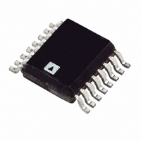
ADT7517ARQZ Analog Devices Inc, ADT7517ARQZ Datasheet - Page 23

ADT7517ARQZ
Manufacturer Part Number
ADT7517ARQZ
Description
IC SENSOR TEMP QD ADC/DAC 16QSOP
Manufacturer
Analog Devices Inc
Datasheet
1.ADT7517ARQZ.pdf
(44 pages)
Specifications of ADT7517ARQZ
Function
Temp Monitoring System (Sensor)
Topology
ADC, Comparator, Multiplexer, Register Bank
Sensor Type
External & Internal
Sensing Temperature
-40°C ~ 120°C, External Sensor
Output Type
I²C™, MICROWIRE™, QSPI™, SPI™
Output Alarm
No
Output Fan
No
Voltage - Supply
2.7 V ~ 5.5 V
Operating Temperature
-40°C ~ 120°C
Mounting Type
Surface Mount
Package / Case
16-QSOP
Ic Output Type
Voltage
Sensing Accuracy Range
± 0.5°C
Supply Current
2.2mA
Supply Voltage Range
2.7V To 5.5V
Resolution (bits)
10bit
Sensor Case Style
QSOP
No. Of Pins
16
Temperature Sensor Function
Temp Sensor
Resolution
10b
Operating Temperature (min)
-40C
Operating Temperature (max)
120C
Operating Supply Voltage (min)
2.7V
Operating Supply Voltage (typ)
3.3/5V
Operating Supply Voltage (max)
5.5V
Lead Free Status / RoHS Status
Lead free / RoHS Compliant
Lead Free Status / RoHS Status
Lead free / RoHS Compliant, Lead free / RoHS Compliant
Available stocks
Company
Part Number
Manufacturer
Quantity
Price
Company:
Part Number:
ADT7517ARQZ
Manufacturer:
Analog Devices Inc
Quantity:
135
FUNCTIONAL DESCRIPTION—ANALOG INPUTS
Single-Ended Inputs
The ADT7516/ADT7517/ADT7519 offer four single-ended
analog input channels. The analog input range is from 0 V to
2.28 V, or 0 V to V
is recommended that the maximum V
Selection between the two input ranges is done by Bit C4 of the
Control Configuration 3 register (Address 0x1A). Setting this
bit to 0 sets up the analog input ADC reference to be sourced
from the internal voltage reference of 2.28 V. Setting the bit to 1
sets up the ADC reference to be sourced from V
The ADC resolution is 10 bits and is mostly suitable for dc
input signals. Bits[C1:C2] of the Control Configuration 1
register (Address 0x18) are used to set up Pin 7 and Pin 8 as
AIN1 and AIN2. Figure 48 shows the overall view of the
4-channel analog input path.
Converter Operation
The analog input channels use a successive approximation ADC
based on a capacitor DAC. Figure 49 and Figure 50 show simpli-
fied schematics of the ADC. Figure 49 shows the ADC during
acquisition phase. SW2 is closed and SW1 is in Position A.
The comparator is held in a balanced condition and the
sampling capacitor acquires the signal on AIN.
When the ADC eventually goes into conversion phase (see
Figure 50), SW2 opens and SW1 moves to Position B, causing
AIN
AIN
REF/2
AIN1
AIN2
AIN3
AIN4
REF/2
SW1
SW1
A
A
Figure 48. Quad Analog Input Path
B
CAPACITOR
Figure 49. ADC Acquisition Phase
CAPACITOR
B
Figure 50. ADC Conversion Phase
SAMPLING
DD
SAMPLING
. To maintain the linearity specification, it
SW2
M
U
R
SW2
L
T
P
L
E
X
E
I
COMPARATOR
COMPARATOR
ACQUISITION
CONVERSION
10-BIT
INT V
ADC
INT V
PHASE
PHASE
REF
REF
DD
CAP DAC
value be set at 5 V.
CONTROL
CAP DAC
CONTROL
TO ADC
VALUE
REGISTER
LOGIC
LOGIC
REF
REF
DD
.
V
V
DD
DD
Rev. B | Page 23 of 44
the comparator to become unbalanced. The control logic and
the DAC are used to add and subtract fixed amounts of charge
from the sampling capacitor to bring the comparator back into
a balanced condition. When the comparator is rebalanced, the
conversion is complete. The control logic generates the ADC
output code. Figure 51 shows the ADC transfer function for the
analog inputs.
ADC TRANSFER FUNCTION
The output coding of the ADT7516/ADT7517/ADT7519 analog
inputs is straight binary. The designed code transitions occur
midway between successive integer LSB values (that is, 1/2 LSB,
3/2 LSB). The LSB is V
V
Figure 51.
To work out the voltage on any analog input channel, the
following method can be used:
Convert value read back from AIN value register into decimal.
where d = decimal.
For example, if internal reference is used, V
AIN value = 512d
Analog Input ESD Protection
Figure 52 shows the input structure on any of the analog input
pins that provide ESD protection. The diode provides the main
ESD protection for the analog inputs. Care must be taken that
the analog input signal never drops below the GND rail by
more than 200 mV. If this happens, the diode becomes forward-
biased and starts conducting current into the substrate. The
4 pF capacitor is the typical pin capacitance and the resistor is a
lumped component made up of the on resistance of the
multiplexer switch.
REF
= 2.28 V. The ideal transfer characteristic is shown in
1 LSB = reference (V)/1024
AIN voltage = AIN value (d) × LSB size
1 LSB size = 2.28 V/1024 = 2.226 × 10
AIN voltage = 512 × 2.226 × 10
000...010
000...001
000...000
111...110
111...000
011...111
111...111
Figure 51. Single-Ended Transfer Function
0V 1/2LSB
ADT7516/ADT7517/ADT7519
DD
/1024 or internal V
ANALOG INPUT
1LSB = INT V
1LSB = V
+V
−3
REF
= 1.14 V
DD
– 1LSB
/1024
REF
−3
REF
REF
/1024
= 2.28 V.
/1024, internal


