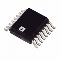
ADT7517ARQZ Analog Devices Inc, ADT7517ARQZ Datasheet - Page 32

ADT7517ARQZ
Manufacturer Part Number
ADT7517ARQZ
Description
IC SENSOR TEMP QD ADC/DAC 16QSOP
Manufacturer
Analog Devices Inc
Datasheet
1.ADT7517ARQZ.pdf
(44 pages)
Specifications of ADT7517ARQZ
Function
Temp Monitoring System (Sensor)
Topology
ADC, Comparator, Multiplexer, Register Bank
Sensor Type
External & Internal
Sensing Temperature
-40°C ~ 120°C, External Sensor
Output Type
I²C™, MICROWIRE™, QSPI™, SPI™
Output Alarm
No
Output Fan
No
Voltage - Supply
2.7 V ~ 5.5 V
Operating Temperature
-40°C ~ 120°C
Mounting Type
Surface Mount
Package / Case
16-QSOP
Ic Output Type
Voltage
Sensing Accuracy Range
± 0.5°C
Supply Current
2.2mA
Supply Voltage Range
2.7V To 5.5V
Resolution (bits)
10bit
Sensor Case Style
QSOP
No. Of Pins
16
Temperature Sensor Function
Temp Sensor
Resolution
10b
Operating Temperature (min)
-40C
Operating Temperature (max)
120C
Operating Supply Voltage (min)
2.7V
Operating Supply Voltage (typ)
3.3/5V
Operating Supply Voltage (max)
5.5V
Lead Free Status / RoHS Status
Lead free / RoHS Compliant
Lead Free Status / RoHS Status
Lead free / RoHS Compliant, Lead free / RoHS Compliant
Available stocks
Company
Part Number
Manufacturer
Quantity
Price
Company:
Part Number:
ADT7517ARQZ
Manufacturer:
Analog Devices Inc
Quantity:
135
ADT7516/ADT7517/ADT7519
Control Configuration 1 Register (Read/Write)
[Address = 0x18]
This configuration register is an 8-bit read/write register that is
used to set up some of the operating modes of the ADT7516/
ADT7517/ADT7519.
Table 15. Control Configuration 1
D7
PD
0
1
Table 16.
Bit
C0
[C1:C2]
C3
C4
C5
C6
PD
Control Configuration 2 Register (Read/Write)
[Address = 0x19]
This configuration register is an 8-bit read/write register that is
used to set up some of the operating modes of the ADT7516/
ADT7517/ADT7519.
D7
C7
0
1
Default settings at power-up.
Default settings at power-up.
1
1
D6
C6
0
D6
C6
0
1
1
Function
This bit enables/disables conversions in round robin
and single-channel mode.
ADT7516/ADT7517/ADT7519 powers up in round
robin mode but monitoring is not initiated until this bit
is set. The default = 0.
Selects between the two different analog inputs on
Pin 7 and Pin 8. ADT7516/ADT7517/ADT7519 powers
up with AIN1 and AIN2 selected.
Selects between digital (LDAC) and analog inputs
(AIN3) on Pin 9. When AIN3 is selected, Bit C3 of the
Control Configuration 3 register is masked and has no
effect until LDAC is selected as the input on Pin 9.
Reserved. Write 0 only.
Configures INT/INT output polarity.
Power-Down Bit. Setting this bit to 1 puts the
ADT7516/ADT7517/ADT7519 into standby mode. In
this mode, both ADC and DACs are fully powered
down, but the serial interface is still operational. To
power up the part again, just write 0 to this bit.
0 = stop monitoring.
1 = start monitoring.
00 = AIN1 and AIN2 selected.
01 = undefined.
10 = external TDM selected.
11 = undefined.
0 = LDAC selected.
1 = AIN3 selected.
0 = enable INT/INT output.
1 = disable INT/INT output.
0 = active low.
1 = active high.
D5
C5
0
D5
C5
0
1
1
D4
C4
0
D4
C4
0
1
1
D3
C3
0
D3
C3
0
1
1
D2
C2
0
D2
C2
0
1
1
D1
C1
0
D1
C1
0
1
1
D0
C0
0
D0
C0
0
1
1
Rev. B | Page 32 of 44
Table 17.
Bit
[C0:C2]
C3
C4
C5
C6
C7
Control Configuration 3 Register (Read/Write)
[Address = 0x1A]
This configuration register is an 8-bit read/write register that is
used to set up some of the operating modes of the ADT7516/
ADT7517/ADT7519.
D7
C7
0
1
Default settings at power-up.
1
D6
C6
0
1
Function
In single-channel mode, these bits select between V
the internal temperature sensor, external temperature
sensor/AIN1, AIN2, AIN3, and AIN4 for conversion. The
default is V
Reserved.
Selects between single-channel and round robin
conversion cycle. The default is round robin.
Default condition is to average every measurement on
all channels 16 times. This bit disables this averaging.
Channels affected are temperature, analog inputs, and
V
SMBus timeout on the serial clock puts a 25 ms limit
on the pulse width of the clock, ensuring that a fault
on the master SCL does not lock up the SDA line.
Software Reset. Setting this bit to 1 causes a software
reset. All registers and DAC outputs reset to their
default settings.
DD
000 = V
001 = internal temperature sensor.
010 = external temperature sensor/AIN1.
(Bits[C1:C2] of the Control Configuration 1 register
affect this selection).
011 = AIN2.
100 = AIN3.
101 = AIN4.
110 to 111 = reserved.
0 = round robin.
1 = single channel.
0 = enable averaging.
1 = disable averaging.
0 = disable SMBus timeout.
1 = enable SMBus timeout.
.
D5
C5
0
1
DD
DD
.
.
D4
C4
0
1
D3
C3
0
1
D2
C2
0
1
D1
C1
0
1
D0
C0
0
1
DD
,


