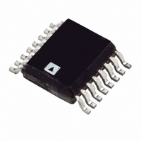
ADT7517ARQZ Analog Devices Inc, ADT7517ARQZ Datasheet - Page 6

ADT7517ARQZ
Manufacturer Part Number
ADT7517ARQZ
Description
IC SENSOR TEMP QD ADC/DAC 16QSOP
Manufacturer
Analog Devices Inc
Datasheet
1.ADT7517ARQZ.pdf
(44 pages)
Specifications of ADT7517ARQZ
Function
Temp Monitoring System (Sensor)
Topology
ADC, Comparator, Multiplexer, Register Bank
Sensor Type
External & Internal
Sensing Temperature
-40°C ~ 120°C, External Sensor
Output Type
I²C™, MICROWIRE™, QSPI™, SPI™
Output Alarm
No
Output Fan
No
Voltage - Supply
2.7 V ~ 5.5 V
Operating Temperature
-40°C ~ 120°C
Mounting Type
Surface Mount
Package / Case
16-QSOP
Ic Output Type
Voltage
Sensing Accuracy Range
± 0.5°C
Supply Current
2.2mA
Supply Voltage Range
2.7V To 5.5V
Resolution (bits)
10bit
Sensor Case Style
QSOP
No. Of Pins
16
Temperature Sensor Function
Temp Sensor
Resolution
10b
Operating Temperature (min)
-40C
Operating Temperature (max)
120C
Operating Supply Voltage (min)
2.7V
Operating Supply Voltage (typ)
3.3/5V
Operating Supply Voltage (max)
5.5V
Lead Free Status / RoHS Status
Lead free / RoHS Compliant
Lead Free Status / RoHS Status
Lead free / RoHS Compliant, Lead free / RoHS Compliant
Available stocks
Company
Part Number
Manufacturer
Quantity
Price
Company:
Part Number:
ADT7517ARQZ
Manufacturer:
Analog Devices Inc
Quantity:
135
ADT7516/ADT7517/ADT7519
Parameter
1
2
3
4
5
6
7
8
9
10
11
12
DAC AC CHARACTERISTICS
V
Table 2.
Parameter
Output Voltage Settling Time
Slew Rate
Major-Code Change Glitch Energy
Digital Feedthrough
Digital Crosstalk
Analog Crosstalk
DAC-to-DAC Crosstalk
Multiplying Bandwidth
Total Harmonic Distortion
1
2
3
See the Terminology section.
DC specifications are tested with the outputs unloaded.
Linearity is tested using a reduced code range: ADT7516 (Code 115 to 4095); ADT7517 (Code 28 to 1023); ADT7519 (Code 8 to 255).
Guaranteed by design and characterization, not production tested.
Round robin is the continuous sequential measurement of the following channels: V
For the amplifier output to reach its minimum voltage, the offset error must be negative. For the amplifier output to reach its maximum voltage (V
plus gain error must be positive.
The SDA and SCL timing is measured with the input filters turned on to meet the fast mode I
but has a negative effect on the EMC behavior of the part.
Guaranteed by design, not production tested. All I
rate specifications.
See the Terminology section.
Guaranteed by design and characterization, not production tested.
At 25°C.
The interface is also capable of handling the I
All input signals are specified with tr = tf = 5 ns (10% to 90% of V
Measured with the load circuit shown in Figure 4.
The I
DD
I
Power Dissipation
ADT7519
ADT7517
ADT7516
DD
= 2.7 V to 5.5 V, R
(Power-Down Mode)
DD
specification is valid for all DAC codes and full-scale analog input voltages. Interface inactive. All DACs and ADCs active. Load currents excluded.
1
1, 2
L
= 4.7 kΩ to GND, C
2
C standard mode rise time specification of 1000 ns.
Min
2
C timing specifications are for fast mode operation but the interface is still capable of handling the slower standard
L
= 200 pF to GND, 4.7 kΩ to V
Min
Typ
DD
Typ
6
7
8
0.7
12
0.5
1
0.5
3
200
–70
), and timed from a voltage level of 1.6 V.
3
Max
10
10
10
33
Rev. B | Page 6 of 44
Max
8
9
10
DD
Unit
μA
μA
mW
μW
, internal temperature, external temperature (AIN1, AIN2), AIN3, and AIN4.
Unit
μs
μs
μs
V/μs
nV-s
nV-s
nV-s
nV-s
nV-s
kHz
dB
DD
2
C specification. Switching off the input filters improves the transfer rate
, all specifications T
Conditions/Comments
V
1/4 scale to 3/4 scale change (0x40 to 0xC0)
1/4 scale to 3/4 scale change (0x100 to 0x300)
1/4 scale to 3/4 scale change (0x400 to 0xC00)
1 LSB change around major carry
V
V
REF
REF
REF
= V
= 2 V ±0.1 V p-p
= 2.5 V ±0.1 V p-p; frequency = 10 kHz
Conditions/Comments
V
V
V
V
DD
DD
DD
DD
DD
= 5 V
= 3.3 V, V
= 5 V, V
= 3.3 V, normal mode
= 3.3 V, shutdown mode
MIN
IH
to T
IH
= V
= V
DD
MAX
DD
, and V
, unless otherwise noted.
, and V
IL
= GND
IL
= GND
REF
= V
DD
), the offset


