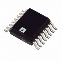
ADT7518ARQ-REEL Analog Devices Inc, ADT7518ARQ-REEL Datasheet - Page 11

ADT7518ARQ-REEL
Manufacturer Part Number
ADT7518ARQ-REEL
Description
IC SENSOR TEMP W/ADC/DAC 16QSOP
Manufacturer
Analog Devices Inc
Datasheet
1.ADT7518ARQ.pdf
(40 pages)
Specifications of ADT7518ARQ-REEL
Rohs Status
RoHS non-compliant
Function
Temp Monitoring System (Sensor)
Topology
ADC, Comparator, Multiplexer, Register Bank
Sensor Type
External & Internal
Sensing Temperature
-40°C ~ 120°C, External Sensor
Output Type
I²C™, MICROWIRE™, QSPI™, SPI™
Output Alarm
No
Output Fan
No
Voltage - Supply
2.7 V ~ 5.5 V
Operating Temperature
-40°C ~ 120°C
Mounting Type
Surface Mount
Package / Case
16-QSOP
DAC-to-DAC Crosstalk
This is the glitch impulse transferred to the output of one DAC
due to a digital code change and subsequent output change of
another DAC. This includes both digital and analog crosstalk. It
is measured by loading one of the DACs with a full-scale code
change (all 0s to all 1s and vice versa) with LDAC low and
monitoring the output of another DAC. The energy of the glitch
is expressed in nV-s.
Multiplying Bandwidth
The amplifiers within the DAC have a finite bandwidth. The
multiplying bandwidth is a measure of this. A sine wave on the
reference (with full-scale code loaded to the DAC) appears on
the output. The multiplying bandwidth is the frequency at
which the output amplitude falls to 3 dB below the input.
Total Harmonic Distortion
This is the difference between an ideal sine wave and its atten-
uated version using the DAC. The sine wave is used as the
reference for the DAC, and the THD is a measure of the
harmonics present on the DAC output, expressed in dB.
Round Robin
This term is used to describe the ADT7518 cycling through the
available measurement channels in sequence, taking a measure-
ment on each channel.
DAC Output Settling Time
This is the time required, following a prescribed data change, for
the output of a DAC to reach and remain within ±0.5 LSB of the
final value. A typical prescribed change is from 1/4 scale to
3/4 scale.
Rev. A | Page 11 of 40
POSITIVE
VOLTAGE
OFFSET
OUTPUT
ERROR
Figure 9. DAC Transfer Function with Positive Offset (V
FOOTROOM
AMPLIFIER
NEGATIVE
NEGATIVE
OFFSET
OFFSET
ERROR
ERROR
VOLTAGE
OUTPUT
Figure 8. DAC Transfer Function with Negative Offset
DEADBAND
LOWER
CODES
DAC CODE
DAC CODE
ACTUAL
IDEAL
OFFSET ERROR
UPPER
DEADBAND
CODES
FULL SCALE
GAIN ERROR
OFFSET ERROR
ACTUAL
IDEAL
GAIN ERROR
+
ADT7518
REF
+
= V
DD
)


