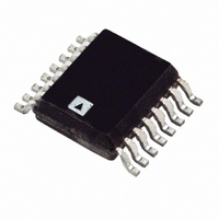
ADT7518ARQ-REEL Analog Devices Inc, ADT7518ARQ-REEL Datasheet - Page 38

ADT7518ARQ-REEL
Manufacturer Part Number
ADT7518ARQ-REEL
Description
IC SENSOR TEMP W/ADC/DAC 16QSOP
Manufacturer
Analog Devices Inc
Datasheet
1.ADT7518ARQ.pdf
(40 pages)
Specifications of ADT7518ARQ-REEL
Rohs Status
RoHS non-compliant
Function
Temp Monitoring System (Sensor)
Topology
ADC, Comparator, Multiplexer, Register Bank
Sensor Type
External & Internal
Sensing Temperature
-40°C ~ 120°C, External Sensor
Output Type
I²C™, MICROWIRE™, QSPI™, SPI™
Output Alarm
No
Output Fan
No
Voltage - Supply
2.7 V ~ 5.5 V
Operating Temperature
-40°C ~ 120°C
Mounting Type
Surface Mount
Package / Case
16-QSOP
ADT7518
SMBus/SPI INT/INT
The ADT7518 INT/ INT output is an interrupt line for devices
that want to trade their ability to master for an extra pin. It is a
slave device and uses the SMBus/SPI INT/ INT to signal the host
device that it wants to talk to. The SMBus/SPI INT/ INT on the
ADT7518 is used as an over/under limit indicator.
The INT/ INT pin has an open-drain configuration that allows
the outputs of several devices to be wired-AND’ed together
when the INT/ INT pin is active low. Use C6 of the Control
Config-uration 1 register to set the active polarity of the
INT/ INT out-put. The power-up default is active low. The
INT/ INT output can be disabled or enabled by setting C5 of the
Control Config-uration 1 register to 1 or 0, respectively.
The INT/ INT output becomes active when either the internal
temperature value, the external temperature value, V
any of the AIN input values exceed the values in their corres-
ponding T
put goes inactive again when a conversion result has the
measured value back within the trip limits and when the status
register associated with the out-of-limit event is read. The two
HIGH
DOUT
SCLK
DIN
CS
SPI
/V
CS
HIGH
START
or T
D7
X
LOW
1
/V
D6
X
LOW
D5
registers. The INT/ INT out-
X
READ OPERATION
READ COMMAND
Figure 62. SPI—Reading Two Bytes of Data From Two Sequential Registers
D4
X
Figure 63. SPI—Correct Use of CS During SPI Communication
DOUT (CONTINUED)
SCLK (CONTINUED)
DIN (CONTINUED)
D3
CS (CONTINUED)
X
D2
DD
X
value, or
D1
X
Rev. A | Page 38 of 40
D0
X
8
X
D7
D7
X
1
1
D6
interrupt status registers show which event caused the INT/ INT
pin to go active.
The INT/ INT output requires an external pull-up resistor. This
can be connected to a voltage different from V
maximum voltage rating of the INT/ INT output pin is not
exceeded. The value of the pull-up resistor depends on the
application but should be large enough to avoid excessive sink
currents at the INT/ INT output, which can heat the chip and
affect the temperature reading.
SMBUS ALERT RESPONSE
The INT/ INT pin behaves the same way as an SMBus alert pin
when the SMBus/I
output and requires a pull-up to V
can be wire-AND’ed together, so that the common line will go
low if one or more of the INT/ INT outputs goes low. The polar-
ity of the INT/ INT pin must be set active low for a number of
outputs to be wire-AND’ed together.
D6
X
X
D5
D5
X
X
DATA BYTE 1
D4
D4
X
DATA BYTE 2
X
WRITE OPERATION
D3
D3
X
X
2
C interface is selected. It is an open-drain
D2
D2
X
X
D1
X
D1
X
D0
D0
X
DD
X
8
8
. Several INT/ INT outputs
STOP
DD
, provided the


