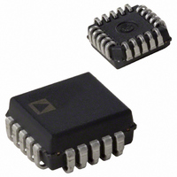
AD652JP Analog Devices Inc, AD652JP Datasheet - Page 14

AD652JP
Manufacturer Part Number
AD652JP
Description
IC V-F CONV SYNCH MONO 5V 20PLCC
Manufacturer
Analog Devices Inc
Type
Voltage to Frequencyr
Datasheet
1.AD652JPZ.pdf
(28 pages)
Specifications of AD652JP
Rohs Status
RoHS non-compliant
Frequency - Max
2MHz
Full Scale
±25ppm/°C
Linearity
±0.005%
Mounting Type
Surface Mount
Package / Case
20-LCC (J-Lead)
Converter Function
VFC
Full Scale Frequency
2000
Power Supply Requirement
Single/Dual
Single Supply Voltage (max)
36V
Single Supply Voltage (min)
12V
Dual Supply Voltage (typ)
±15V
Dual Supply Voltage (min)
±6V
Dual Supply Voltage (max)
±18V
Operating Temperature (min)
0C
Operating Temperature (max)
70C
Operating Temperature Classification
Commercial
Package Type
PLCC
Lead Free Status / Rohs Status
Not Compliant
Available stocks
Company
Part Number
Manufacturer
Quantity
Price
Part Number:
AD652JP
Manufacturer:
ADI/亚德诺
Quantity:
20 000
Company:
Part Number:
AD652JP-REEL
Manufacturer:
Analog Devices Inc
Quantity:
10 000
Company:
Part Number:
AD652JP-REEL7
Manufacturer:
Analog Devices Inc
Quantity:
10 000
Part Number:
AD652JPZ
Manufacturer:
ADI/亚德诺
Quantity:
20 000
AD652
SINGLE-SUPPLY OPERATION
In addition to the Digital Ground being connected to –V
also possible to connect Analog Ground to –V
Thus, the device is truly operating from a single-supply voltage
that can range from 12 V to 36 V. This is shown in Figure 21 for
a positive voltage input, and in Figure 20 for a negative voltage
input.
In Figure 21, the comparator reference is used as a derived
ground; the input voltage is referred to this point as well as to
the op amp common mode (Pin 6 is tied to Pin 16). Since the
input signal source must drive 0.5 mA of full-scale signal
current into Pin 7, it must also draw the exact same current
from the input reference potential. This current is therefore
provided by the 5 V reference.
In single-supply operation, an external resistor, R
necessary between the power supply, +V
SOURCE
REFERENCE
SIGNAL
REFERENCE
SIGNAL
SOURCE
1V FULL SCALE
INPUT
INPUT
+
–
+
–
I
FULL SCALE
SIGNAL
I
0.5mA
SIGNAL
2kΩ
S
, and the 5 V reference
C
C
INT
INT
ANALOG
GND
+V
S
Figure 20. Single-Supply Mode Negative Voltage Input
+V
Figure 21. Single-Supply Mode Positive Voltage Input
of the AD652.
S
S
PULLUP
R
1
2
3
4
5
6
7
8
R
PULLUP
1
2
3
4
5
6
7
8
PULLUP
20kΩ
20kΩ
SYNCHRONOUS
VOLTAGE-TO-
SYNCHRONOUS
, is
FREQUENCY
CONVERTER
VOLTAGE-TO-
FREQUENCY
CONVERTER
AD652
1mA
S
AD652
, it is
1mA
Rev. C | Page 14 of 28
REFERENCE
AND
REFERENCE
AND
5V
output. This resistor should be selected such that a current of
approximately 500 µA flows during operation. For example,
with a power supply voltage of +15 V, a 20 kΩ resistor is selected
((15 V–5 V)/500 µA = 20 kΩ).
Figure 20 shows the negative voltage input configuration for
using the AD652 in single-supply mode. In this mode, the signal
source is driving the + input of the op amp, which requires only
20 nA (typical) compared to the 0.5 mA required in the positive
input voltage configuration. The voltage at Pin 6 may go as low
as 4 V above ground (−V
V above ground, this leaves a 1 V window for the input signal.
To drive the integrating capacitor with a 0.5 mA full-scale
current, it is necessary to provide an external 2 kΩ resistor. This
results in a 2 kΩ resistor and a 1 V input range. The external
2 kΩ resistor should be a low TC metal-film type for lowest
drift degradation.
5V
D
SHOT
ONE
D
Q
Q
SHOT
ONE
Q
Q
FLOP
"D"
FLOP
CK
"D"
CK
16
15
14
13
12
11
10
9
16
15
14
13
12
11
10
9
R
R
L
ANALOG
GND
L
ANALOG
GND
CLOCK
CLOCK
C
OS
5V
5V
C
S
OS
Pin 8). Since the input reference is 5.0
DIGITAL
GND
FREQ
OUT
DIGITAL
GND


