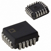
AD652JP Analog Devices Inc, AD652JP Datasheet - Page 21

AD652JP
Manufacturer Part Number
AD652JP
Description
IC V-F CONV SYNCH MONO 5V 20PLCC
Manufacturer
Analog Devices Inc
Type
Voltage to Frequencyr
Datasheet
1.AD652JPZ.pdf
(28 pages)
Specifications of AD652JP
Rohs Status
RoHS non-compliant
Frequency - Max
2MHz
Full Scale
±25ppm/°C
Linearity
±0.005%
Mounting Type
Surface Mount
Package / Case
20-LCC (J-Lead)
Converter Function
VFC
Full Scale Frequency
2000
Power Supply Requirement
Single/Dual
Single Supply Voltage (max)
36V
Single Supply Voltage (min)
12V
Dual Supply Voltage (typ)
±15V
Dual Supply Voltage (min)
±6V
Dual Supply Voltage (max)
±18V
Operating Temperature (min)
0C
Operating Temperature (max)
70C
Operating Temperature Classification
Commercial
Package Type
PLCC
Lead Free Status / Rohs Status
Not Compliant
Available stocks
Company
Part Number
Manufacturer
Quantity
Price
Part Number:
AD652JP
Manufacturer:
ADI/亚德诺
Quantity:
20 000
Company:
Part Number:
AD652JP-REEL
Manufacturer:
Analog Devices Inc
Quantity:
10 000
Company:
Part Number:
AD652JP-REEL7
Manufacturer:
Analog Devices Inc
Quantity:
10 000
Part Number:
AD652JPZ
Manufacturer:
ADI/亚德诺
Quantity:
20 000
Analog Signal Reconstruction
If it is desired to reconstruct the analog voltages from the
multiplex signal, three more AD652 SVFC devices are used as
frequency-to-voltage converters, as shown in Figure 31. The
comparator inputs of all the devices are strapped together, the
“+” inputs are held at a 1.2 V TTL threshold, and the “−” inputs
are driven by the multiplex input. The three clock inputs are
10kΩ
AD589
1.2V
V
V
IN
VOLTS
LO
OUT
+5V
HI
V
2
6.8kΩ
0.02µF
1.5kΩ
1.2kΩ
–V
+V
S
S
1
2
3
4
5
6
7
8
7915
10kΩ
1
2
3
4
SYNCHRONOUS
VOLTAGE-TO-
FREQUENCY
CONVERTER
AD652
–15V
–15V
REG
DRIVER
OSC
AD654
1N4148
7
47µF
47µF
φ
2,
6
φ
Figure 31. Demultiplexer Frequency-to-Voltage Conversion
16
15
14
13
12
11
10
3,
9
5
1N4148
φ
47µF
47µF
+5V
8
7
6
5
4 ARE PINS 15, 7, 6 OF TIM9904A FROM DEMUX FIGURE 30
4kΩ
φ
4
T50- MICROMETALS
2
+15V
+15V
REG
VOLTS
200pF
OUT
Figure 32. Isolated Synchronous VFC
V
24 TURNS
3
0.02µF
7815
–V
+V
S
100Ω
1.65kΩ
Rev. C | Page 21 of 28
S
1
2
3
4
5
6
7
8
0.02µF
SYNCHRONOUS
VOLTAGE-TO-
FREQUENCY
CONVERTER
2N6659
AD652
1
CK
MYLAR
0.01µF
2
Q
–15V
+5V
+15V
'74
driven by the ϕ outputs of the clock chip. Remember that data
at the comparator input of the SVFC is loaded on the falling
edge of the clock signal and shifted out on the next rising edge.
Note that the frequency signals for each data channel are
available at the frequency output pin of each FVC.
10µH
2N6659
Q
D
1
2
3
4
5
6
7
8
3
20kΩ
16
15
14
13
12
11
10
9
SYNCHRONOUS
TRANSFORMER
MPX INPUT
1.65kΩ
VOLTAGE-TO-
FREQUENCY
CONVERTER
PICO 31080
100Ω
AD652
1mA
φ
3
VOLTS
OUT
V
ISOLATION BARRIER
CK
4
0.02µF
500Ω
'74
–V
1nF
+V
S
+5V
S
Q
D
REFERENCE
1
2
3
4
5
6
7
8
AND
SYNCHRONOUS
5
6
7
8
5V
VOLTAGE-TO-
FREQUENCY
CONVERTER
D
AD652
SHOT
ONE
Q
Q
ISOLATOR
OPTO-
FLOP
6N137
"D"
CK
16
15
14
13
12
11
10
9
16
15
14
13
12
11
10
9
4
3
2
1
FREQUENCY
OUTPUT
3kΩ
φ
4
1kΩ
1nF
AD652


