AD652JP Analog Devices Inc, AD652JP Datasheet - Page 4
AD652JP
Manufacturer Part Number
AD652JP
Description
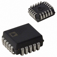
IC V-F CONV SYNCH MONO 5V 20PLCC
Manufacturer
Analog Devices Inc
Type
Voltage to Frequencyr
Datasheet
1.AD652JPZ.pdf
(28 pages)
Specifications of AD652JP
Rohs Status
RoHS non-compliant
Frequency - Max
2MHz
Full Scale
±25ppm/°C
Linearity
±0.005%
Mounting Type
Surface Mount
Package / Case
20-LCC (J-Lead)
Converter Function
VFC
Full Scale Frequency
2000
Power Supply Requirement
Single/Dual
Single Supply Voltage (max)
36V
Single Supply Voltage (min)
12V
Dual Supply Voltage (typ)
±15V
Dual Supply Voltage (min)
±6V
Dual Supply Voltage (max)
±18V
Operating Temperature (min)
0C
Operating Temperature (max)
70C
Operating Temperature Classification
Commercial
Package Type
PLCC
Lead Free Status / Rohs Status
Not Compliant
Available stocks
Company
Part Number
Manufacturer
Quantity
Price

Part Number:
AD652JP
Manufacturer:
ADI/亚德诺
Quantity:
20 000
Company:
Part Number:
AD652JP-REEL
Manufacturer:
Analog Devices Inc
Quantity:
10 000
Company:
Part Number:
AD652JP-REEL7
Manufacturer:
Analog Devices Inc
Quantity:
10 000
Part Number:
AD652JPZ
Manufacturer:
ADI/亚德诺
Quantity:
20 000


AD652
Parameter
COMPARATOR
CLOCK INPUT
OUTPUT STAGE
OUTPUT ONE-SHOT
REFERENCE OUTPUT
POWER SUPPLY
TEMPERATURE RANGE
1
Referred to internal V
Input Bias Current
Common-Mode Voltage
Maximum Frequency
Threshold Voltage (Referred to Pin 12)
Input Current
Voltage Range
Rise Time
V
I
I
Delay Time, Positive Clock Edge to Output Pulse
Fall Time (Load = 500 pF and I
Output Capacitance
Pulse Width, t
Voltage
Drift
Output Current
Power Supply Rejection
Output Impedance (Sourcing Current)
Rated Voltage
Operating Range
Quiescent Current
Digital Common
Analog Common
Specified Performance
OL
OH
OL
T
(−V
V
V
C
C
Source T
Sink
Supply Range = ±12.5 V to ±17.5 V
Dual Supply
Single Supply (−V
JP, KP Grade
AQ, BQ Grade
SQ Grade
(Off Leakage)
MIN
(I
OL
OL
OS
OS
OUT
S
< 0.8 V
< 0.4 V, T
= 300 pF
= 1000 pF
to T
< V
= 10 mA)
CLK
MAX
MIN
< +V
OS
to T
MIN
REF
to T
MAX
S
. In PLCC package, tested on 10 V input range only.
)
S
MAX
= 0)
SINK
= 5 mA)
Min
−V
4
0.8
−V
150
1
4
4.950
10
100
±6
+12
−V
−V
0
−40
−55
S
S
S
S
Rev. C | Page 4 of 28
+ 4
AD652JP/AQ/SQ
Typ
0.5
5
1.2
5
0.01
200
100
5
1.5
5
5.0
500
0.3
±15
±15
±11
Max
5
+ V
2.0
20
+V
2
0.4
15
8
10
250
2
6
5.050
100
0.015
2
±18
+36
±15
+V
+V
+70
+85
+125
S
S
S
S
− 4
− 4
Min
−V
4
0.8
−V
150
1
4
4.975
10
100
±6
+12
–V
−V
0
−40
S
S
S
S
+ 4
AD652KP/BQ
Typ
5
5
0.01
200
100
5
1.5
5
5.0
0.3
±11
0.5
1.2
500
±15
±15
Max
5
+V
2.0
20
+V
2
0.4
15
8
10
250
2
6
5.025
50
0.015
2
±18
+36
±15
+V
+V
+70
+85
S
S
S
S
− 4
− 4
Unit
µA
V
MHz
V
V
µA
V
µs
V
mA
mA
µA
ns
ns
pF
µs
µs
V
ppm/°C
mA
µA
%/V
Ω
V
V
V
mA
V
V
°C
°C
°C
Related parts for AD652JP
Image
Part Number
Description
Manufacturer
Datasheet
Request
R

Part Number:
Description:
±1.7g Dual-Axis IMEMS Accelerometer Evaluation Board
Manufacturer:
Analog Devices Inc
Datasheet:

Part Number:
Description:
Inertial Sensor Evaluation System
Manufacturer:
Analog Devices Inc
Datasheet:
Part Number:
Description:
Manufacturer:
Analog Devices Inc
Datasheet:
Part Number:
Description:
Manufacturer:
Analog Devices Inc
Datasheet:
Part Number:
Description:
Manufacturer:
Analog Devices Inc
Datasheet:
Part Number:
Description:
Manufacturer:
Analog Devices Inc
Datasheet:
Part Number:
Description:
Manufacturer:
Analog Devices Inc
Datasheet:
Part Number:
Description:
Manufacturer:
Analog Devices Inc
Datasheet:
Part Number:
Description:
Manufacturer:
Analog Devices Inc
Datasheet:
Part Number:
Description:
Manufacturer:
Analog Devices Inc
Datasheet:
Part Number:
Description:
Manufacturer:
Analog Devices Inc
Datasheet:
Part Number:
Description:
Manufacturer:
Analog Devices Inc
Datasheet:
Part Number:
Description:
Manufacturer:
Analog Devices Inc
Datasheet: