AD652JP Analog Devices Inc, AD652JP Datasheet - Page 20
AD652JP
Manufacturer Part Number
AD652JP
Description
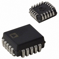
IC V-F CONV SYNCH MONO 5V 20PLCC
Manufacturer
Analog Devices Inc
Type
Voltage to Frequencyr
Datasheet
1.AD652JPZ.pdf
(28 pages)
Specifications of AD652JP
Rohs Status
RoHS non-compliant
Frequency - Max
2MHz
Full Scale
±25ppm/°C
Linearity
±0.005%
Mounting Type
Surface Mount
Package / Case
20-LCC (J-Lead)
Converter Function
VFC
Full Scale Frequency
2000
Power Supply Requirement
Single/Dual
Single Supply Voltage (max)
36V
Single Supply Voltage (min)
12V
Dual Supply Voltage (typ)
±15V
Dual Supply Voltage (min)
±6V
Dual Supply Voltage (max)
±18V
Operating Temperature (min)
0C
Operating Temperature (max)
70C
Operating Temperature Classification
Commercial
Package Type
PLCC
Lead Free Status / Rohs Status
Not Compliant
Available stocks
Company
Part Number
Manufacturer
Quantity
Price

Part Number:
AD652JP
Manufacturer:
ADI/亚德诺
Quantity:
20 000
Company:
Part Number:
AD652JP-REEL
Manufacturer:
Analog Devices Inc
Quantity:
10 000
Company:
Part Number:
AD652JP-REEL7
Manufacturer:
Analog Devices Inc
Quantity:
10 000
Part Number:
AD652JPZ
Manufacturer:
ADI/亚德诺
Quantity:
20 000


AD652
SVFC Demultiplexer
The demultiplexer needed to separate the combined signals is
shown in Figure 30. A phase-locked loop drives another 4-phase
clock chip to lock onto the reconstructed clock signal. The sync
pulses are distinguished from the data pulses by their shorter
duration. Each falling edge on the multiplex input signal
triggers the one-shot; at the end of this one-shot pulse, the
multiplex input signal is sampled by a D-type flip-flop. If the
signal is high, the pulse was short (a sync pulse) and the Q
output of the D-flop goes low. The D-flop is cleared a short time
(two gate delays) later, and the clock is reconstructed as a
stream of short, low-going pulses. If the multiplex input is a data
pulse, then the signal will still be low and no pulse will appear at
the reconstructed clock output when the D-flop samples at the
end of the one-shot period. See Figure 29.
If it is desired to recover the individual frequency signals, the
multiplex input is sampled with a D-flop at the appropriate
time, as determined by the rising edge of the various phases
generated by the clock chip. These frequency signals can be
counted as a ratio relative to the reconstructed clock, so it is not
even necessary for the transmitter to be crystal-controlled as
shown in Figure 30.
INPUT
MPX
f2
D
Q
CLOCK
'74 (1/2)
+5V
CLOCK
D
GND
FREQUENCY OUTPUTS
NC
A1
A2
RECONSTRUCTED
Q
Q
1/2 '74
φ
2
1
2
3
4
5
6
7
CLEAR
RECONSTRUCTED
f3
D
Q
CLOCK OUTPUT
CLOCK
Q
ONE SHOT
'74 (1/2)
Q
'00
'00
'121
Q
φ
3
Figure 30. SVFC Demultiplexers
14
13
12
11
10
9
8
f4
D
Q
CLOCK
'74 (1/2)
V
NC
NC
R
C
R
NC
Rev. C | Page 20 of 28
CC
EXT
EXT
INT
/C
1
3
50pF
+5V
EXT
2kΩ
14
4
PHASE LOCK LOOP
390pF
+5V
φ
4
13
2
MC4044
φ
φ
150Ω
3
4
130Ω
4
11
5
10
1
2
3
4
5
6
7
8
9
TANK 1
TANK 2
GND 1
FFQ
FFD
φ
φ
φ
φ
GND 2
8
4 PHASE CLOCK
10
4 TTL
3 TTL
3
4
9
TIM 9904A
NC = NO CONNECT
+5V
SYNC
3.01kΩ
719Ω
1kΩ
φ
0.1µF
1
OSCOUT
Figure 29. Demultiplexer Waveforms
XTAL 2
XTAL 1
φ
φ
Figure 28. Multiplexer Waveforms
OSCIN
2 TTL
1 TTL
V
V
2
CC
DD
φ
φ
1
2
3
6
φ
+5V
20
19
18
17
16
15
14
13
12
11
'LS629
2
16
VCO
8
+5V
DATA
15
9
φ
φ
φ
3
1
2
11
7
4
5
50pF
φ
4
MULTIPLEX
INPUT
ONE SHOT
RECONSTRUCTED
CLOCK
φ
(PHASE LOCKED TO
RECONSTRUCTED
CLOCK)
1
φ
φ
φ
φ
1MULTIPLEX
OUTPUT
1
2
3
4
Related parts for AD652JP
Image
Part Number
Description
Manufacturer
Datasheet
Request
R

Part Number:
Description:
±1.7g Dual-Axis IMEMS Accelerometer Evaluation Board
Manufacturer:
Analog Devices Inc
Datasheet:

Part Number:
Description:
Inertial Sensor Evaluation System
Manufacturer:
Analog Devices Inc
Datasheet:
Part Number:
Description:
Manufacturer:
Analog Devices Inc
Datasheet:
Part Number:
Description:
Manufacturer:
Analog Devices Inc
Datasheet:
Part Number:
Description:
Manufacturer:
Analog Devices Inc
Datasheet:
Part Number:
Description:
Manufacturer:
Analog Devices Inc
Datasheet:
Part Number:
Description:
Manufacturer:
Analog Devices Inc
Datasheet:
Part Number:
Description:
Manufacturer:
Analog Devices Inc
Datasheet:
Part Number:
Description:
Manufacturer:
Analog Devices Inc
Datasheet:
Part Number:
Description:
Manufacturer:
Analog Devices Inc
Datasheet:
Part Number:
Description:
Manufacturer:
Analog Devices Inc
Datasheet:
Part Number:
Description:
Manufacturer:
Analog Devices Inc
Datasheet:
Part Number:
Description:
Manufacturer:
Analog Devices Inc
Datasheet: