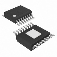
ISL6268CAZ Intersil, ISL6268CAZ Datasheet - Page 12

ISL6268CAZ
Manufacturer Part Number
ISL6268CAZ
Description
IC PWM CTRLR SYNC BUCK 16-QSOP
Manufacturer
Intersil
Datasheet
1.ISL6268CAZ.pdf
(14 pages)
Specifications of ISL6268CAZ
Pwm Type
Controller
Number Of Outputs
1
Frequency - Max
600kHz
Voltage - Supply
7 V ~ 25 V
Buck
Yes
Boost
No
Flyback
No
Inverting
No
Doubler
No
Divider
No
Cuk
No
Isolated
No
Operating Temperature
-10°C ~ 100°C
Package / Case
16-QSOP
Frequency-max
600kHz
Lead Free Status / RoHS Status
Lead free / RoHS Compliant
Duty Cycle
-
Available stocks
Company
Part Number
Manufacturer
Quantity
Price
Part Number:
ISL6268CAZ
Manufacturer:
INTERSIL
Quantity:
20 000
Part Number:
ISL6268CAZ-T
Manufacturer:
INTERSIL
Quantity:
20 000
MOSFET Selection and Considerations
Typically, a MOSFET cannot tolerate even brief excursions
beyond their maximum drain to source voltage rating. The
MOSFETs used in the power stage of the converter should
have a maximum V
upper voltage tolerance of the input power source and the
voltage spike that occurs when the MOSFET switches off.
There are several power MOSFETs readily available that are
optimized for DC/DC converter applications. The preferred
high-side MOSFET emphasizes low switch charge so that
the device spends the least amount of time dissipating
power in the linear region. Unlike the low-side MOSFET
which has the drain-source voltage clamped by its body
diode during turn off, the high-side MOSFET turns off with
V
emphasizes low r
conduction loss.
For the low-side MOSFET, (LS), the power loss can be
assumed to be conductive only and is written as:
For the high-side MOSFET, (HS), its conduction loss is
written as:
For the high-side MOSFET, its switching loss is written as:
where:
- I
- I
- T
- T
Selecting The Bootstrap Capacitor
The selection of the bootstrap capacitor is written as:
where:
- Q
- ∆V
P
P
P
C
IN
CON_LS
CON_HS
SW_HS
BOOT
inductor current minus half of the inductor ripple current
current plus half of the inductor ripple current
high-side MOSFET
the boot capacitor each time the high-side MOSFET is
switched on
VALLEY
PEAK
ON
OFF
- V
g
BOOT
is the total gate charge required to turn on the
OUT
is the time required to drive the device into saturation
=
is the time required to drive the device into cut-off
is the sum of the DC component of the inductor
=
≈
----------------------- -
∆V
=
, is the maximum allowed voltage decay across
- V
is the difference of the DC component of the
I
V
-------------------------------------------------------------------- -
LOAD
I
IN
Q
BOOT
LOAD
L
g
•
across it. The preferred low-side MOSFET
I
VALLEY
2
DS(on)
2
r ⋅
DS
•
DS on
r
DS on
rating that exceeds the sum of the
2
(
(
•
when fully saturated to minimize
T
)_LS
ON
)_HS
12
•
•
F
(
SW
•
1 D
D
–
+
)
V
---------------------------------------------------------------- -
IN
•
I
PEAK
2
•
T
OFF
(EQ. 18)
(EQ. 16)
(EQ. 17)
(EQ. 19)
•
F
SW
ISL6268
As an example, suppose the high-side MOSFET has a total
gate charge Q
200mV. The calculated bootstrap capacitance is 0.125µF.
For a comfortable margin, select a capacitor that is double
the calculated capacitance; in this example, 0.22µF will
suffice. Use an X7R or X5R ceramic capacitor.
Layout Considerations
As a general rule, power should be on the bottom layer of
the PCB and weak analog or logic signals are on the top
layer of the PCB. The ground-plane layer should be adjacent
to the top layer to provide shielding. The ground plane layer
should have an island located under the IC, the
compensation components, and the FSET components. The
island should be connected to the rest of the ground plane
layer at one point.
Signal Ground and Power Ground
The GND pin is the signal ground for analog and logic
signals of the IC. For a robust thermal and electrical
conduction path, connect the GND pin to the island of
ground plane under the top layer using several vias.
Connect the input capacitors, the output capacitors, and the
source of the lower MOSFETs to the power ground plane.
PGND (Pin 12)
This is the return path for the pull-down of the LG low-side
MOSFET gate driver. Ideally, PGND should be connected to
the source of the low-side MOSFET with a low-resistance,
low-inductance path.
VIN (Pin 3)
The VIN pin should be connected close to the drain of the
high-side MOSFET, using a low resistance and low
inductance path.
VCC (Pin 4)
For best performance, place the decoupling capacitor very
close to the VCC and GND pins.
PVCC (Pin 14)
For best performance, place the decoupling capacitor very
close to the PVCC and PGND pins, preferably on the same
side of the PCB as the ISL6268 IC.
FIGURE 7. TYPICAL POWER COMPONENT PLACEMENT
INDUCTOR
HIGH-SIDE
MOSFETS
GROUND
VIAS TO
g
PLANE
of 25nC at V
PHASE
NODE
VOUT
GND
VIN
GS
OUTPUT
CAPACITORS
= 5V, and a ∆V
SCHOTTKY
DIODE
LOW-SIDE
MOSFETS
INPUT
CAPACITORS
BOOT
August 22, 2006
of
FN6348.0


